Datasheet 搜索 > MOS管 > TI(德州仪器) > CSD17483F4T 数据手册 > CSD17483F4T 其他数据使用手册 1/14 页

¥ 1.751
CSD17483F4T 其他数据使用手册 - TI(德州仪器)
制造商:
TI(德州仪器)
分类:
MOS管
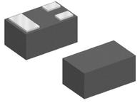
封装:
PICOSTAR-3
描述:
TEXAS INSTRUMENTS CSD17483F4T 晶体管, MOSFET, N沟道, 1.5 A, 30 V, 0.185 ohm, 8 V, 850 mV
Pictures:
3D模型
符号图
焊盘图
引脚图
产品图
页面导航:
导航目录
CSD17483F4T数据手册
Page:
of 14 Go
若手册格式错乱,请下载阅览PDF原文件
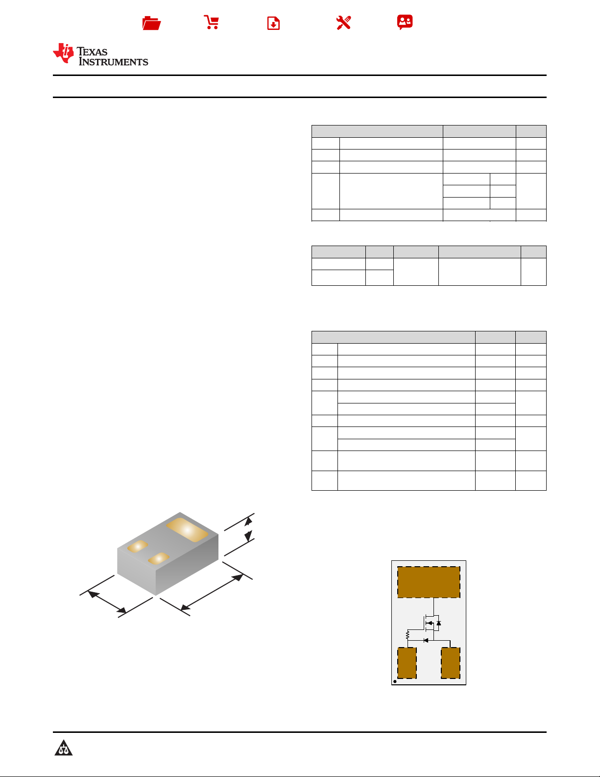
D
G S
0.60 mm
1.00 mm
0.35 mm
Product
Folder
Sample &
Buy
Technical
Documents
Tools &
Software
Support &
Community
An IMPORTANT NOTICE at the end of this data sheet addresses availability, warranty, changes, use in safety-critical applications,
intellectual property matters and other important disclaimers. PRODUCTION DATA.
CSD17483F4
SLPS447D –JULY 2013–REVISED DECEMBER 2016
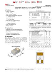
CSD17483F4 30-V N-Channel FemtoFET™ MOSFET
1
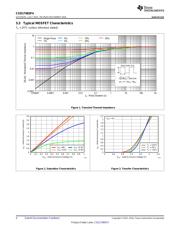
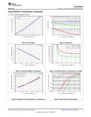
1 Features
1
• Low On Resistance
• Low Q
g
and Q
gd
• Low-Threshold Voltage
• Ultra-Small Footprint (0402 Case Size)
– 1.0 mm × 0.6 mm
• Ultra-Low Profile
– 0.35-mm Height
• Integrated ESD Protection Diode
– Rated > 4-kV HBM
– Rated > 2-kV CDM
• Lead and Halogen Free
• RoHS Compliant
2 Applications
• Optimized for Load Switch Applications
• Optimized for General Purpose Switching
Applications
• Single-Cell Battery Applications
• Handheld and Mobile Applications
3 Description
This 200-mΩ, 30-V N-Channel FemtoFET™
MOSFET technology is designed and optimized to
minimize the footprint in many handheld and mobile
applications. This technology is capable of replacing
standard small signal MOSFETs while providing at
least a 60% reduction in footprint size.
.
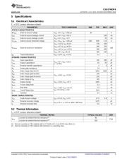
Typical Part Dimensions
.
.
.
.
Product Summary
T
A
= 25°C TYPICAL VALUE UNIT
V
DS
Drain-to-Source Voltage 30 V
Q
g
Gate Charge Total (4.5 V) 1010 pC
Q
gd
Gate Charge Gate-to-Drain 130 pC
R
DS(on)
Drain-to-Source
On Resistance
V
GS
= 1.8 V 370
mΩV
GS
= 2.5 V 240
V
GS
= 4.5 V 200
V
GS(th)
Threshold Voltage 0.85 V
Device Information
(1)
DEVICE QTY MEDIA PACKAGE SHIP
CSD17483F4 3000
7-Inch Reel
Femto(0402)
1.00 mm × 0.60 mm
SMD Lead Less
Tape
and
Reel
CSD17483F4T 250
(1) For all available packages, see the orderable addendum at
the end of the data sheet.
Absolute Maximum Ratings
T
A
= 25°C unless otherwise stated VALUE UNIT
V
DS
Drain-to-Source Voltage 30 V
V
GS
Gate-to-Source Voltage 12 V
I
D
Continuous Drain Current, T
A
= 25°C
(1)
1.5 A
I
DM
Pulsed Drain Current, T
A
= 25°C
(2)
5 A
I
G
Continuous Gate Clamp Current 35
mA
Pulsed Gate Clamp Current
(2)
350
P
D
Power Dissipation
(1)
500 mW
V
(ESD)
Human-Body Model (HBM) 4
kV
Charged-Device Model (CDM) 2
T
J
,
T
stg
Operating Junction,
Storage Temperature
–55 to 150 °C
E
AS
Avalanche Energy, Single Pulse I
D
= 7.4 A,
L = 0.1 mH, R
G
= 25 Ω
2.7 mJ
(1) Typical R
θJA
= 90°C/W on 1-in
2
(6.45-cm
2
), 2-oz
(0.071-mm) thick Cu pad on a 0.06-in (1.52-mm) thick FR4
PCB.
(2) Pulse duration ≤ 300 μs, duty cycle ≤ 2%.
Top View
器件 Datasheet 文档搜索
AiEMA 数据库涵盖高达 72,405,303 个元件的数据手册,每天更新 5,000 多个 PDF 文件
