Datasheet 搜索 > MOS管 > TI(德州仪器) > CSD18540Q5B 数据手册 > CSD18540Q5B 其他数据使用手册 1/15 页

¥ 5.246
CSD18540Q5B 其他数据使用手册 - TI(德州仪器)
制造商:
TI(德州仪器)
分类:
MOS管
封装:
VSON-Clip-8
描述:
60V、N 通道 NexFET(TM) 功率 MOSFET
Pictures:
3D模型
符号图
焊盘图
引脚图
产品图
页面导航:
导航目录
CSD18540Q5B数据手册
Page:
of 15 Go
若手册格式错乱,请下载阅览PDF原文件
0
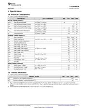
0.5
1
1.5
2
2.5
3
3.5
4
4.5
5
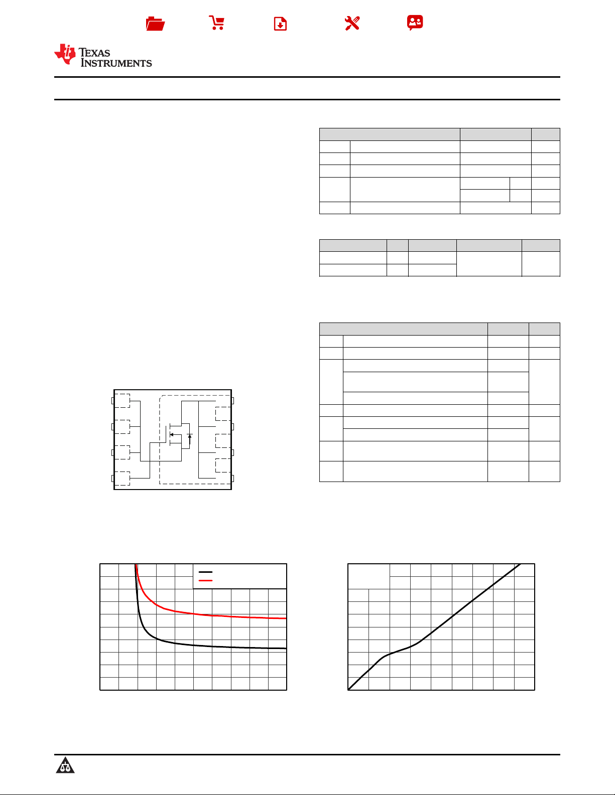
0 2 4 6 8 10 12 14 16 18 20
V
GS
- Gate-to- Source Voltage (V)
R
DS(on)
- On-State Resistance (mΩ)
T
C
= 25°C, I
D
= 28A
T
C
= 125°C, I
D
= 28A
G001
0
1
2
3
4
5
6
7
8
9
10
0 5 10 15 20 25 30 35 40 45
Q
g
- Gate Charge (nC)
V
GS
- Gate-to-Source Voltage (V)
I
D
= 28A
V
DS
= 30V
G001
1
D
2
D
3
D
4
D
D
5
G
6S
7
S
8S
P0093-01
Product
Folder
Sample &
Buy
Technical
Documents
Tools &
Software
Support &
Community
CSD18540Q5B
SLPS488 –JUNE 2014
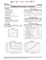
CSD18540Q5B 60V N-Channel NexFET™ Power MOSFETs
1 Features
Product Summary
1
• Ultra-Low Q
g
and Q
gd
T
A
= 25°C TYPICAL VALUE UNIT
• Low Thermal Resistance
V
DS
Drain-to-Source Voltage 60 V
• Avalanche Rated
Q
g
Gate Charge Total (10 V) 41 nC
Q
gd
Gate Charge Gate-to-Drain 6.7 nC
• Pb-Free Terminal Plating
V
GS
= 4.5 V 2.6 mΩ
• RoHS Compliant
R
DS(on)
Drain-to-Source On Resistance
V
GS
= 10 V 1.8 mΩ
• Halogen Free
V
GS(th)
Threshold Voltage 1.9 V
• SON 5-mm × 6-mm Plastic Package
Ordering Information
(1)
2 Applications
Device Qty Media Package Ship
• DC-DC Conversion
CSD18540Q5B 2500 13-Inch Reel
SON 5 × 6 mm Tape and
Plastic Package Reel
• Secondary Side Synchronous Rectifier
CSD18540Q5BT 250 7-Inch Reel
• Isolated Converter Primary Side Switch
(1) For all available packages, see the orderable addendum at
the end of the data sheet.
• Motor Control
Absolute Maximum Ratings
3 Description
T
A
= 25°C VALUE UNIT
This 1.8 mΩ, 60 V, SON5x6 NexFET™ power
V
DS
Drain-to-Source Voltage 60 V
MOSFET is designed to minimize losses in power
V
GS
Gate-to-Source Voltage ±20 V
conversion applications.
Continuous Drain Current (Package limited) 100
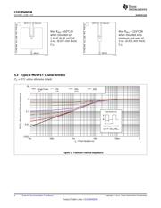
Top View
Continuous Drain Current (Silicon limited),
I
D
221 A
T
C
= 25°C
Continuous Drain Current
(1)
28
I
DM
Pulsed Drain Current, T
A
= 25°C
(2)
400 A
Power Dissipation
(1)
3.1
P
D
W
Power Dissipation, T
C
= 25°C 195
T
J
, Operating Junction and
–55 to 150 °C
T
stg
Storage Temperature Range
Avalanche Energy, single pulse
E
AS
320 mJ
I
D
= 80 A, L = 0.1 mH, R
G
= 25 Ω
(1) Typical R
θJA
= 40°C/W on a 1-inch
2
, 2-oz. Cu pad on a 0.06-
inch thick FR4 PCB.
(2) Max R
θJC
= 0.8°C/W, Pulse duration ≤100 μs, duty cycle ≤1%
R
DS(on)
vs V
GS
Gate Charge
1
An IMPORTANT NOTICE at the end of this data sheet addresses availability, warranty, changes, use in safety-critical applications,
intellectual property matters and other important disclaimers. PRODUCTION DATA.
器件 Datasheet 文档搜索
AiEMA 数据库涵盖高达 72,405,303 个元件的数据手册,每天更新 5,000 多个 PDF 文件
