Datasheet 搜索 > MOS管 > TI(德州仪器) > CSD85301Q2 数据手册 > CSD85301Q2 其他数据使用手册 1/16 页

¥ 1.54
CSD85301Q2 其他数据使用手册 - TI(德州仪器)
制造商:
TI(德州仪器)
分类:
MOS管
封装:
WSON-FET-6
描述:
CSD85301Q2,双路 N 通道 NexFET™ 功率 MOSFET
Pictures:
3D模型
符号图
焊盘图
引脚图
产品图
页面导航:
导航目录
CSD85301Q2数据手册
Page:
of 16 Go
若手册格式错乱,请下载阅览PDF原文件
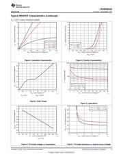
V
GS
- Gate-to-Source Voltage (V)
R
DS(on)
- On-State Resistance (m:)
0 2 4 6 8 10
0
10
20
30
40
50
60
70
D007
T
C
= 25°C, I
D
= 5 A
T
C
= 125°C, I
D
= 5 A
Q
g
- Gate Charge (nC)
V
GS
- Gate-to-Source Voltage (V)
0 0.5 1 1.5 2 2.5 3 3.5 4 4.5 5
0
0.5
1
1.5
2
2.5
3
3.5
4
4.5
5
D004
I
D
= 5 A
V
DS
= 10 V
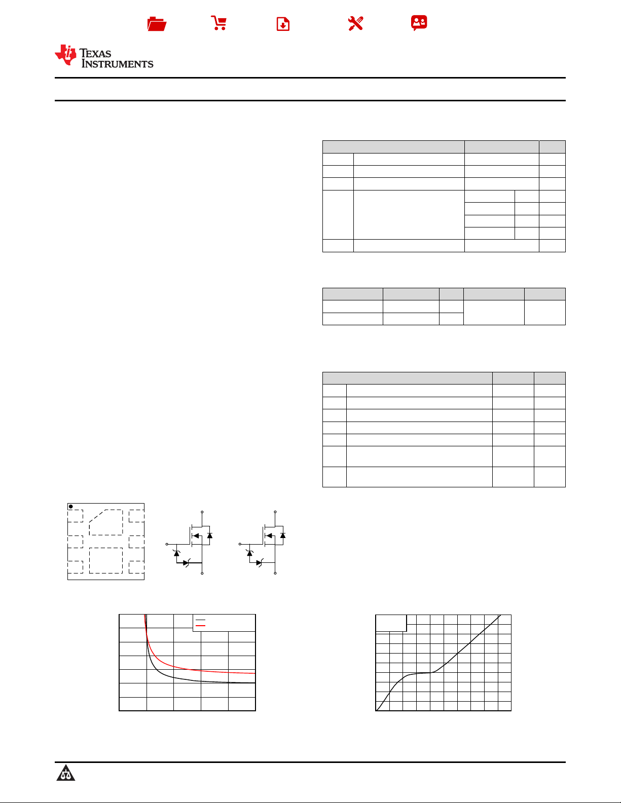
S1
G1
D2
D2
D1
G2
S2
D1
Drain
Gate
Source
Drain
Gate
Source
Product
Folder
Sample &
Buy
Technical
Documents
Tools &
Software
Support &
Community
CSD85301Q2
SLPS521 –DECEMBER 2014
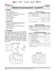
CSD85301Q2 20 V Dual N-Channel NexFET™ Power MOSFETs
.
1 Features
1
• Low On-Resistance
Product Summary
• Dual Independent MOSFETs
T
A
= 25°C TYPICAL VALUE UNIT
• Space Saving SON 2 × 2 mm Plastic Package
V
DS
Drain-to-Source Voltage 20 V
Q
g
Gate Charge Total (4.5 V) 4.2 nC
• Optimized for 5 V Gate Driver
Q
gd
Gate Charge Gate to Drain 1.0 nC
• Avalanche Rated
V
GS
= 1.8 V 65 mΩ
• Pb and Halogen Free
V
GS
= 2.5 V 33 mΩ
R
DS(on)
Drain-to-Source On Resistance
• RoHS Compliant
V
GS
= 3.8 V 25 mΩ
V
GS
= 4.5 V 23 mΩ
2 Applications
V
GS(th)
Threshold Voltage 0.9 V
• Point-of-Load Synchronous Buck Converter for
Applications in Networking, Telecom, and
.
Computing Systems
Ordering Information
(1)
Device Media Qty Package Ship
• Adaptor or USB Input Protection for Notebook
CSD85301Q2 7-Inch Reel 3000
PCs and Tablets
SON 2 x 2 mm Tape and
Plastic Package Reel
CSD85301Q2T 7-Inch Reel 250
• Battery Protection
(1) For all available packages, see the orderable addendum at
the end of the data sheet.
3 Description
The CSD85301Q2 is a 20 V, 23 mΩ N-Channel
Absolute Maximum Ratings
device with dual independent MOSFETs in a SON 2 x
T
A
= 25°C VALUE UNIT
2 mm plastic package. The two FETs were designed
V
DS
Drain-to-Source Voltage 20 V
to be used in a half bridge configuration for
V
GS
Gate-to-Source Voltage ±10 V
synchronous buck and other power supply
applications. Additionally, this part can be used for
I
D
Continuous Drain Current (Package limited) 5.0 A
adaptor, USB input protection and battery charging
I
DM
Pulsed Drain Current
(1)
26 A
applications. The dual FETs feature low drain to
P
D
Power Dissipation
(2)
2.3 W
source on-resistance that minimizes losses and offers
T
J
, Operating Junction and
–55 to 150 °C
low component count for space constrained
T
stg
Storage Temperature Range
applications.
Avalanche Energy, single pulse
E
AS
3.8 mJ
I
D
= 8.7 A, L = 0.1 mH, R
G
= 25 Ω
Top View and Circuit Image
(1) Max R
θJA
= 185 °C/W, pulse duration ≤100 μs, duty cycle
≤1%.
(2) Typical R
θJA
= 55 °C/W on a 1 inch
2
, 2 oz. Cu pad on a 0.06
inch thick FR4 PCB.
R
DS(on)
vs V
GS
Gate Charge
1
An IMPORTANT NOTICE at the end of this data sheet addresses availability, warranty, changes, use in safety-critical applications,
intellectual property matters and other important disclaimers. PRODUCTION DATA.
器件 Datasheet 文档搜索
AiEMA 数据库涵盖高达 72,405,303 个元件的数据手册,每天更新 5,000 多个 PDF 文件
