Datasheet 搜索 > DA转换器 > TI(德州仪器) > DAC161S055CISQ/NOPB 数据手册 > DAC161S055CISQ/NOPB 其他数据使用手册 1/28 页

¥ 3.245
DAC161S055CISQ/NOPB 其他数据使用手册 - TI(德州仪器)
制造商:
TI(德州仪器)
分类:
DA转换器
封装:
WFQFN-16
描述:
DAC161S055精密16位,缓冲电压输出DAC DAC161S055 Precision 16-Bit, Buffered Voltage-Output DAC
Pictures:
3D模型
符号图
焊盘图
引脚图
产品图
页面导航:
引脚图在P2P3P4Hot
原理图在P2
封装尺寸在P23P24P25
标记信息在P23
封装信息在P23P24P25
功能描述在P15
技术参数、封装参数在P1P4P6
应用领域在P1P20P27
电气规格在P4P6P7P8P12P13P14P15
导航目录
DAC161S055CISQ/NOPB数据手册
Page:
of 28 Go
若手册格式错乱,请下载阅览PDF原文件
DAC161S055
www.ti.com
SNAS503B –NOVEMBER 2010–REVISED JANUARY 2012
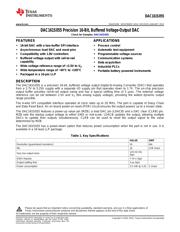
DAC161S055 Precision 16-Bit, Buffered Voltage-Output DAC
Check for Samples: DAC161S055
1
FEATURES
APPLICATIONS
2
• 16-bit DAC with a two-buffer SPI interface
• Process control
• Asynchronous load DAC and reset pins • Automatic test equipment
• Compatibility with 1.8V controllers • Programmable voltage sources
• Buffered voltage output with rail-to-rail • Communication systems
capability
• Data acquisition
• Wide voltage reference range of +2.5V to V
A
• Industrial PLCs
• Wide temperature range of −40°C to +105°C
• Portable battery powered instruments
• Packaged in a 16-pin LLP
DESCRIPTION
The DAC161S055 is a precision 16-bit, buffered voltage output Digital-to-Analog Converter (DAC) that operates
from a 2.7V to 5.25V supply with a separate I/O supply pin that operates down to 1.7V. The on-chip precision
output buffer provides rail-to-rail output swing and has a typical settling time of 5 µsec. The external voltage
reference can be set between 2.5V and V
A
(the analog supply voltage), providing the widest dynamic output
range possible.
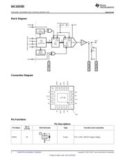
The 4-wire SPI compatible interface operates at clock rates up to 20 MHz. The part is capable of Diasy Chain
and Data Read Back. An on board power-on-reset (POR) circuit ensures the output powers up to a known state.
The DAC161S055 features a power-up value pin (MZB), a load DAC pin (LDACB) and a DAC clear (CLRB) pin.
MZB sets the startup output voltage to either GND or mid-scale. LDACB updates the output, allowing multiple
DACs to update their outputs simultaneously. CLRB can be used to reset the output signal to the value
determined by MZB.
The DAC161S055 has a power-down option that reduces power consumption when the part is not in use. It is
available in a 16-lead LLP package.
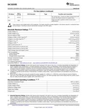
Table 1. Key Specifications
VALUE UNIT
Resolution (guaranteed monotonic) 16 bits
INL ±3 LSB (max)
120 nV/√Hz
Very low output noise
(typ)
Glitch impulse 7 nV-s (typ)
Output settling time 5 µs (typ)
Power consumption 5.5 mW @ 5.25 V (max)
1
Please be aware that an important notice concerning availability, standard warranty, and use in critical applications of
Texas Instruments semiconductor products and disclaimers thereto appears at the end of this data sheet.
2All trademarks are the property of their respective owners.
PRODUCTION DATA information is current as of publication date.
Copyright © 2010–2012, Texas Instruments Incorporated
Products conform to specifications per the terms of the Texas
Instruments standard warranty. Production processing does not
necessarily include testing of all parameters.
器件 Datasheet 文档搜索
AiEMA 数据库涵盖高达 72,405,303 个元件的数据手册,每天更新 5,000 多个 PDF 文件
