Datasheet 搜索 > DA转换器 > ADI(亚德诺) > DAC8412FPCZ 数据手册 > DAC8412FPCZ 其他数据使用手册 1/20 页
 器件3D模型
¥ 152.233
DAC8412FPCZ 其他数据使用手册 - ADI(亚德诺)
制造商:
ADI(亚德诺)
分类:
DA转换器
封装:
PLCC-28
描述:
ANALOG DEVICES DAC8412FPCZ 芯片, 数模转换器
Pictures:
3D模型
符号图
焊盘图
引脚图
产品图
页面导航:
导航目录
DAC8412FPCZ数据手册
Page:
of 20 Go
若手册格式错乱,请下载阅览PDF原文件
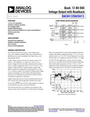
Quad, 12-Bit DAC
Voltage Output with Readback
Data Sheet
DAC8412/DAC8413
FEATURES
+5 V to ±15 V operation
Unipolar or bipolar operation
True voltage output
Double-buffered inputs
Reset to minimum (DAC8413) or center scale (DAC8412)
Fast bus access time
Readback
APPLICATIONS
Automatic test equipment
Digitally controlled calibration
Servo controls
Process control equipment
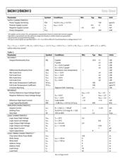
FUNCTIONAL BLOCK DIAGRAM
DGND
A0
A1
CS
RESET
LDAC
12
I/O
PORT
CONTROL
LOGIC
DATA
I/O
R/W
INPUT
REG A
INPUT
REG B
INPUT
REG C
INPUT
REG D
OUTPUT
REG A
OUTPUT
REG B
OUTPUT
REG C
OUTPUT
REG D
DAC A
DAC B
DAC C
DAC D
V
LOGIC
V
DD
V
REFH
V
REFL
V
SS
V
OUTA
V
OUTB
V
OUTC
V
OUTD
00274-001
Figure 1.
GENERAL DESCRIPTION
The DAC8412/DAC8413 are quad, 12-bit voltage output
DACs with readback capability. Built using a complementary
BiCMOS process, these monolithic DACs offer the user very
high package density.
Output voltage swing is set by the two reference inputs V
REFH
and V
REFL
. By setting the V
REFL
input to 0 V and V
REFH
to a
positive voltage, the DAC provides a unipolar positive output
range. A similar configuration with V
REFH
at 0 V and V
REFL
at a
negative voltage provides a unipolar negative output range.
Bipolar outputs are configured by connecting both V
REFH
and
V
REFL
to nonzero voltages. This method of setting output voltage
range has advantages over other bipolar offsetting methods
because it is not dependent on internal and external resistors
with different temperature coefficients.
Digital controls allow the user to load or read back data from any
DAC, load any DAC, and transfer data to all DACs at one time.
An active low
RESET
loads all DAC output registers to midscale
for the DAC8412 and zero scale for the DAC8413.
The DAC8412/DAC8413 are available in 28-lead plastic DIP,
28-lead cerami c DI P, 28-lead PLCC, and 28-lead LCC packages.
They can be operated from a wide variety of supply and reference
voltages with supplies ranging from single +5 V to ±15 V, and
references from +2.5 V to ±10 V. Power dissipation is less than
330 mW with ±15 V supplies and only 60 mW with a +5 V supply.
For MIL-STD-883 applications, contact your local Analog
Devices, Inc. sales office for the DAC8412/DAC8413/883 data
sheet, which specifies operation over the −55°C to +125°C
temperature range. All 883 parts are also available on Standard
Military Drawings 5962-91 76401MXA through 76404M3A.
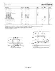
DIGITAL INPUT CODE (Decimal)
0.500
0.125
512
LINEARITY ERROR (LSB)
0.375
–0.125
–0.250
–0.375
–0.500
0.250
0
+125°C
+25°C
–55°C
V
DD
= +15V
V
SS
= –15V
V
REFH
= +10V
V
REFL
= –10V
T
A
= –55°C, +25°C, +125°C
1024 1536 2046 2548 2560 3072 40960
00274-002
Figure 2. INL vs. Code Over Temperature
Rev. G Document Feedback
Information furnished by Analog Devices is believed to be accurate and reliable. However, no
responsibility is assumed by Analog Devices for its use, nor for any infringements of patents or other
rights of third parties that may result from its use. Specifications subject to change without notice. No
license is granted by implication or otherwise under any patent or patent rights of Analog Devices.
Trademarks and registered trademarks are the property of their respective owners.
One Technology Way, P.O. Box 9106, Norwood, MA 02062-9106, U.S.A.
Tel: 781.329.4700 ©2000–2013 Analog Devices, Inc. All rights reserved.
Technical Support www.analog.com
器件 Datasheet 文档搜索
AiEMA 数据库涵盖高达 72,405,303 个元件的数据手册,每天更新 5,000 多个 PDF 文件
