Datasheet 搜索 > 开发套件 > TI(德州仪器) > DRV8805EVM 数据手册 > DRV8805EVM 其他数据使用手册 6/59 页

¥ 854.16
DRV8805EVM 其他数据使用手册 - TI(德州仪器)
制造商:
TI(德州仪器)
分类:
开发套件
描述:
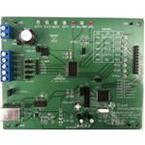
TEXAS INSTRUMENTS DRV8805EVM 评估模块, MSP430处理器, DRV8805
Pictures:
3D模型
符号图
焊盘图
引脚图
产品图
页面导航:
引脚图在P3P4P5P27Hot
典型应用电路图在P15P45P46
原理图在P13P23
封装尺寸在P54P56P57
标记信息在P54
封装信息在P54P55P56P57
技术参数、封装参数在P6
电气规格在P8P9
导航目录
DRV8805EVM数据手册
Page:
of 59 Go
若手册格式错乱,请下载阅览PDF原文件
6
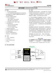
DRV8308
ZHCSC39A –FEBRUARY 2014–REVISED OCTOBER 2014
www.ti.com.cn
Copyright © 2014, Texas Instruments Incorporated
(1) Stresses beyond those listed under “absolute maximum ratings” may cause permanent damage to the device. These are stress ratings
only, and functional operation of the device at these or any other conditions beyond those indicated under “recommended operating
conditions” is not implied. Exposure to absolute–maximum–rated conditions for extended periods may affect device reliability.
(2) All voltage values are with respect to network ground terminal.
(3) Power dissipation and thermal limits must be observed
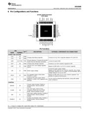
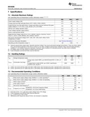
7 Specifications
7.1 Absolute Maximum Ratings
over operating free-air temperature (unless otherwise noted)
(1) (2) (3)
MIN MAX UNIT
Power supply voltage (VM) –0.3 42 V
Charge pump and high side gate drivers (VCP, UHSG, VHSG, WHSG) –0.3 50 V
Output terminal, low side gate drivers, charge pump flying cap and switched VM power
supply voltage (U, V, W, ULSG, VLSG, WLSG, CP1, CP2 VSW)
–0.6 40 V
Internal core voltage regulator (VINT) –0.3 2 V
Linear voltage regulator output (VREG) –0.3 5.5 V
Sense current terminal (ISEN) –0.3 2 V
Digital terminal voltage range (SCLK, SCS, SMODE, SDATAI, SDATAO, FGOUT,
FAULTn, LOCKn, CLKIN, BRAKE, DIR, ENABLE, RESET)
–0.5 5.75 V
Hall sensor input terminal voltage (UHP, UHN, VHP, VHN, WHP, WHN, FGFB,
FGINN/TACH, FGINP)
0 VREG V
Continuous total power dissipation See Thermal Information
Operating junction temperature range, T
J
–40 150 °C
(1) JEDEC document JEP155 states that 500-V HBM allows safe manufacturing with a standard ESD control process.
(2) JEDEC document JEP157 states that 250-V CDM allows safe manufacturing with a standard ESD control process.
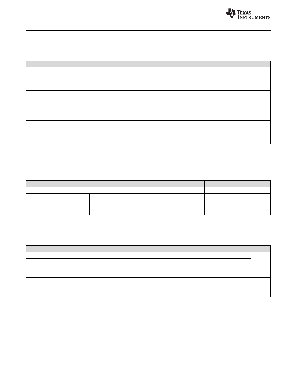
7.2 Handling Ratings
MIN MAX UNIT
T
stg
Storage temperature range –60 150 °C
V
(ESD)
Electrostatic discharge
Human body model (HBM), per ANSI/ESDA/JEDEC JS-001, all
pins
(1)
-4000 4000
V
Charged device model (CDM), per JEDEC specification
JESD22-C101, all pins
(2)
-1500 1500
(1) Note that at VM < 12 V, gate drive output voltage tracks VM voltage
(2) Power dissipation and thermal limits must be observed
(3) f
HALL
of 50 Hz to 6.7 kHz is best
(4) Operational with frequencies above 50 kHz, but resolution is degraded
7.3 Recommended Operating Conditions
over operating free-air temperature range (unless otherwise noted)
MIN NOM MAX UNIT
V
M
Motor power supply voltage range, ENABLE = 1, motor operating
(1)
8.5 32
V
V
MDIS
Motor power supply voltage range, ENABLE = 0, motor not operating 4.5 35
I
VREG
VREG output current
(2)
0 30
mA
I
VSW
VSW output current
(2)
0 30
f
HALL
Hall sensor input frequency
(3)
0 30
kHz
f
CLKIN
Frequency on CLKIN
SPDMODE = 00 (Clock Frequency Mode) 0 90
SPDMODE = 01 (Clock PWM Mode) 16 50
(4)
器件 Datasheet 文档搜索
AiEMA 数据库涵盖高达 72,405,303 个元件的数据手册,每天更新 5,000 多个 PDF 文件
