Datasheet 搜索 > 实时时钟芯片 > Maxim Integrated(美信) > DS1340U3 数据手册 > DS1340U3 其他数据使用手册 1/16 页


¥ 0
DS1340U3 其他数据使用手册 - Maxim Integrated(美信)
制造商:
Maxim Integrated(美信)
分类:
实时时钟芯片
Pictures:
3D模型
符号图
焊盘图
引脚图
产品图
页面导航:
导航目录
DS1340U3数据手册
Page:
of 16 Go
若手册格式错乱,请下载阅览PDF原文件
DS1340
I
2
C RTC with Trickle Charger
________________________________________________________________
Maxim Integrated Products
1
For pricing, delivery, and ordering information, please contact Maxim Direct at 1-888-629-4642,
or visit Maxim’s website at www.maxim-ic.com.
General Description
The DS1340 is a real-time clock (RTC)/calendar that is
pin compatible and functionally equivalent to the ST
M41T00, including the software clock calibration. The
device additionally provides trickle-charge capability
on the V
BACKUP
pin, a lower timekeeping voltage, and
an oscillator STOP flag. Block access of the register
map is identical to the ST device. Two additional regis-
ters, which are accessed individually, are required for
the trickle charger and flag. The clock/calendar pro-
vides seconds, minutes, hours, day, date, month, and
year information. A built-in power-sense circuit detects
power failures and automatically switches to the back-
up supply. Reads and writes are inhibited while the
clock continues to run. The device is programmed seri-
ally through an I
2
C bidirectional bus.
Applications
Portable Instruments
Point-of-Sale Equipment
Medical Equipment
Telecommunications
Features
♦ Enhanced Second Source for the ST M41T00
♦ Available in a Surface-Mount Package with an
Integrated Crystal (DS1340C)
♦ Fast (400kHz) I
2
C Interface
♦ Software Clock Calibration
♦ RTC Counts Seconds, Minutes, Hours, Day, Date,
Month, and Year
♦ Automatic Power-Fail Detect and Switch Circuitry
♦ Trickle-Charge Capability
♦ Low Timekeeping Voltage Down to 1.3V
♦ Three Operating Voltage Ranges (1.8V, 3V, and 3.3V)
♦ Oscillator Stop Flag
♦ Available in 8-Pin µSOP or SO Packages
♦ Underwriters Laboratories (UL) Recognized
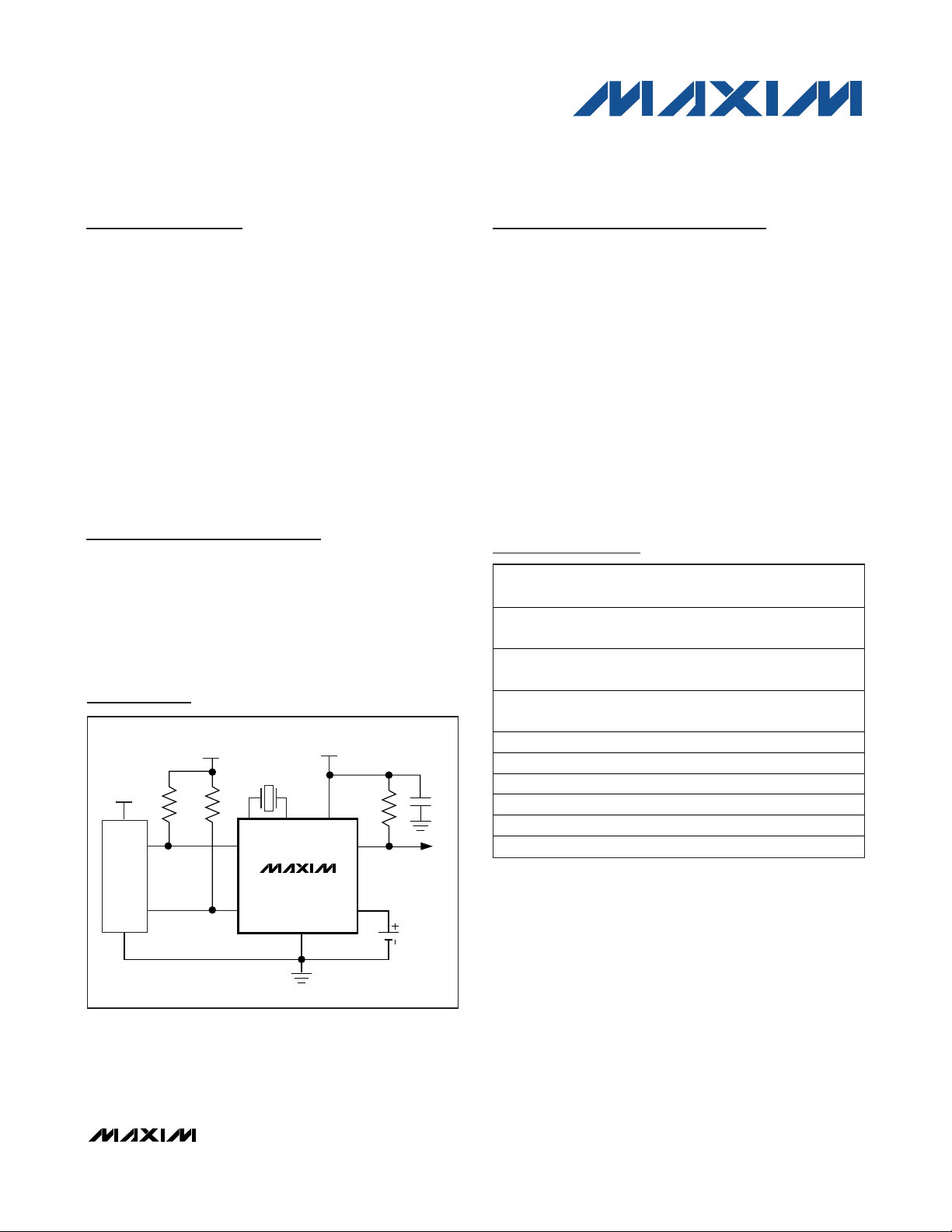
Ordering Information
4
CPU
V
CC
V
CC
V
CC
5
6
8
12
SDA
SCL
GND
X2X1
V
CC
C1
R
PU
R
PU
CRYSTAL
FT/OUT
V
BACKUP
3
7
R
PU
= t
R
/ C
B
DS1340
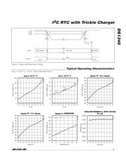
Typical Operating Circuit
PART TEMP RANGE
PIN-
PACKAGE
TOP MARK
†
DS1340Z-18+ -40°C to +85°C
8 SO
(0.150in)
D1340-18
DS1340Z-3+ -40°C to +85°C
8 SO
(0.150in)
DS1340-3
DS1340Z-33+ -40°C to +85°C
8 SO
(0.150in)
D134033
DS1340U-18+ -40°C to +85°C 8 μSOP 1340 -18
DS1340U-3+ -40°C to +85°C 8 μSOP 1340 -3
DS1340U-33+ -40°C to +85°C 8 μSOP 1340 -33
DS1340C-18# -40°C to +85°C 16 SO DS1340C-18
DS1340C-3# -40°C to +85°C 16 SO DS1340C-3
DS1340C-33# -40°C to +85°C 16 SO DS1340C-33
Pin Configurations appear at end of data sheet.
+
Denotes a lead(Pb)-free/RoHS-compliant package.
#
Denotes a RoHS-compliant device that may include lead(Pb)
that is exempt under RoHS requirements. The lead finish is
JESD97 category e3, and is compatible with both lead-based
and lead-free soldering processes.
†
A "+" anywhere on the top mark denotes a lead(Pb)-free device.
A "#" denotes a RoHS-compliant device.
19-5578; Rev 7; 8/11
器件 Datasheet 文档搜索
AiEMA 数据库涵盖高达 72,405,303 个元件的数据手册,每天更新 5,000 多个 PDF 文件
