Datasheet 搜索 > 温度传感器 > Maxim Integrated(美信) > DS18S20-PAR+T&R 数据手册 > DS18S20-PAR+T&R 其他数据使用手册 6/21 页

¥ 23.036
DS18S20-PAR+T&R 其他数据使用手册 - Maxim Integrated(美信)
制造商:
Maxim Integrated(美信)
分类:
温度传感器
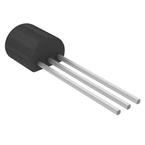
封装:
TO-92-3
描述:
板上安装温度传感器 Prgmble Resolution 1-Wire Parasite Pwr
Pictures:
3D模型
符号图
焊盘图
引脚图
产品图
页面导航:
导航目录
DS18S20-PAR+T&R数据手册
Page:
of 21 Go
若手册格式错乱,请下载阅览PDF原文件
DS18S20-PAR
6 of 20
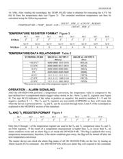
DS18S20-PAR MEMORY MAP Figure 6
SCRATCHPAD (Power-up State)
byte 0 Temperature LSB (AAh)
byte 1 Temperature MSB (00h)
EEPROM
byte 2 T
H
Register or User Byte 1* T
H
Register or User Byte 1
byte 3 T
L
Register or User Byte 2* T
L
Register or User Byte 2
byte 4 Reserved (FFh)
byte 5 Reserved (FFh)
byte 6 COUNT REMAIN (0Ch)
byte 7 COUNT PER °C (10h)
byte 8 CRC*
*Power-up state depends on value(s) stored
in EEPROM
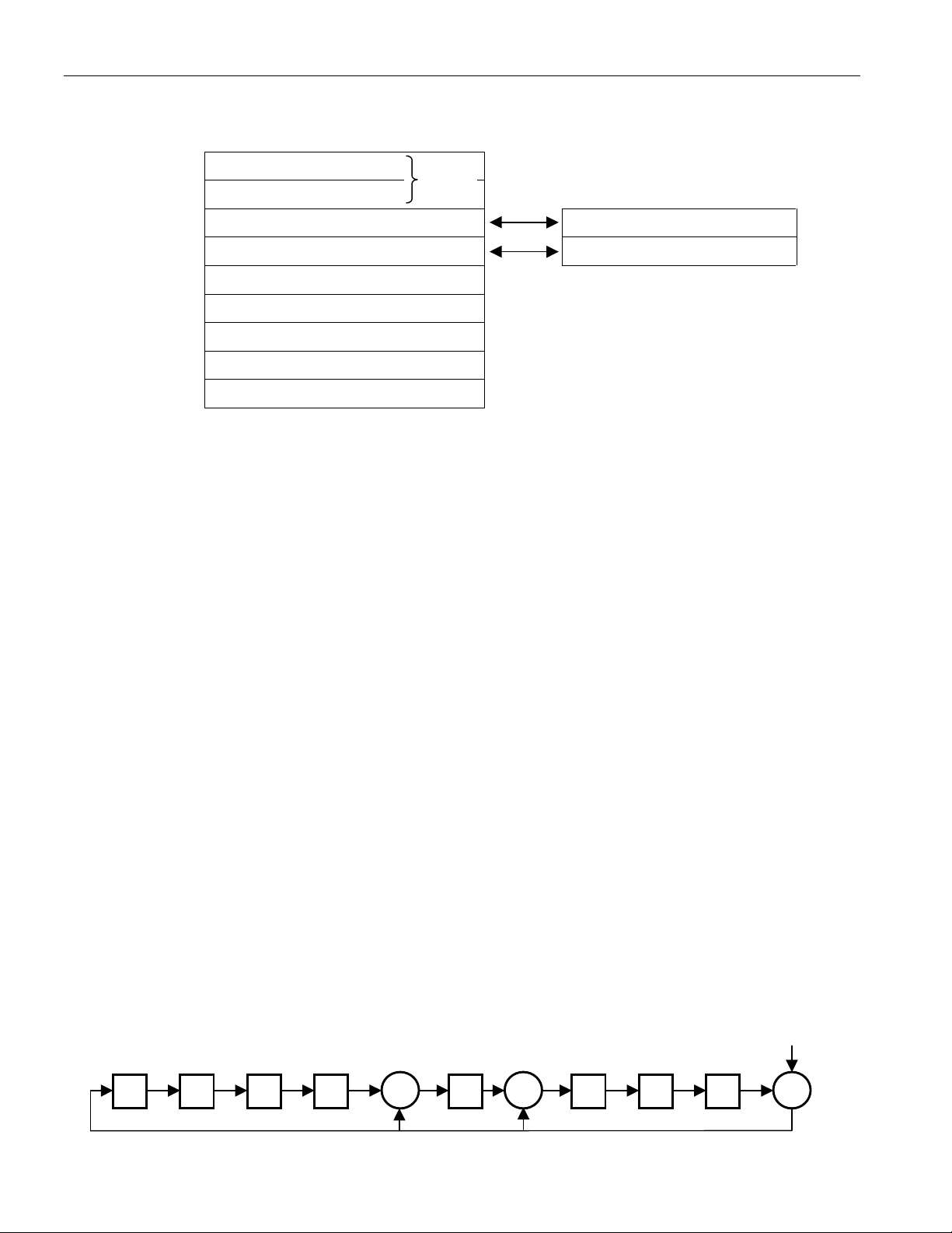
CRC GENERATION
CRC bytes are provided as part of the DS18S20-PAR’s 64-bit ROM code and in the 9
th
byte of the
scratchpad memory. The ROM code CRC is calculated from the first 56 bits of the ROM code and is
contained in the most significant byte of the ROM. The scratchpad CRC is calculated from the data
stored in the scratchpad, and therefore it changes when the data in the scratchpad changes. The CRCs
provide the bus master with a method of data validation when data is read from the DS18S20-PAR. To
verify that data has been read correctly, the bus master must re-calculate the CRC from the received data
and then compare this value to either the ROM code CRC (for ROM reads) or to the scratchpad CRC (for
scratchpad reads). If the calculated CRC matches the read CRC, the data has been received error free. The
comparison of CRC values and the decision to continue with an operation are determined entirely by the
bus master. There is no circuitry inside the DS18S20-PAR that prevents a command sequence from
proceeding if the DS18S20-PAR CRC (ROM or scratchpad) does not match the value generated by the
bus master.
The equivalent polynomial function of the CRC (ROM or scratchpad) is: CRC = X
8
+ X
5
+ X
4
+ 1
The bus master can re-calculate the CRC and compare it to the CRC values from the DS18S20-PAR
using the polynomial generator shown in Figure 7. This circuit consists of a shift register and XOR gates,
and the shift register bits are initialized to 0. Starting with the least significant bit of the ROM code or the
least significant bit of byte 0 in the scratchpad, one bit at a time should shifted into the shift register.
After shifting in the 56
th
bit from the ROM or the most significant bit of byte 7 from the scratchpad, the
polynomial generator will contain the re-calculated CRC. Next, the 8-bit ROM code or scratchpad CRC
from the DS18S20-PAR must be shifted into the circuit. At this point, if the re-calculated CRC was
correct, the shift register will contain all 0s. Additional information about the Dallas 1-Wire cyclic
redundancy check is available in Application Note 27 entitled “Understanding and Using Cyclic
Redundancy Checks with Dallas Semiconductor Touch Memory Products.”
CRC GENERATOR Figure 7
(MSB) (LSB)
XOR XOR
XOR
INPUT
(85°C)
器件 Datasheet 文档搜索
AiEMA 数据库涵盖高达 72,405,303 个元件的数据手册,每天更新 5,000 多个 PDF 文件
