Datasheet 搜索 > 接口芯片 > TI(德州仪器) > DS92LX2121SQX/NOPB 数据手册 > DS92LX2121SQX/NOPB 其他数据使用手册 1/40 页
 器件3D模型
¥ 78.839
DS92LX2121SQX/NOPB 其他数据使用手册 - TI(德州仪器)
制造商:
TI(德州仪器)
分类:
接口芯片
封装:
WQFN-40
描述:
10 - 50MHz 直流平衡信道链路 III 双向控制串行器 40-WQFN -40 to 85
Pictures:
3D模型
符号图
焊盘图
引脚图
产品图
页面导航:
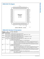
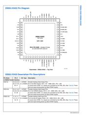
引脚图在P3P5P37Hot
典型应用电路图在P35P36
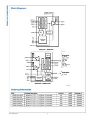
原理图在P2P21
封装尺寸在P38
型号编码规则在P2
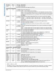
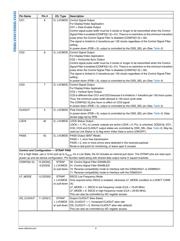
功能描述在P1P21P23P32P33P34
技术参数、封装参数在P9P10P11P15
应用领域在P1P4P7P35
电气规格在P9P10P15
导航目录
DS92LX2121SQX/NOPB数据手册
Page:
of 40 Go
若手册格式错乱,请下载阅览PDF原文件
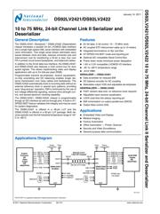
DS92LV2421/DS92LV2422
January 14, 2011
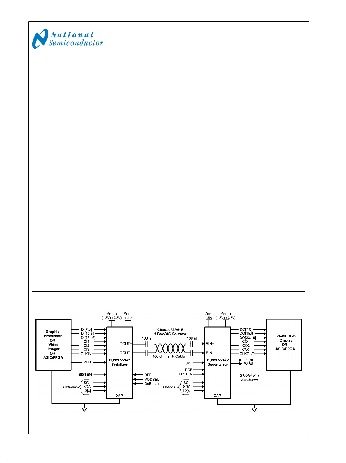
10 to 75 MHz, 24-bit Channel Link II Serializer and
Deserializer
General Description
The DS92LV2421 (Serializer) / DS92LV2422 (Deserializer)
chipset translates a parallel 24–bit LVCMOS data interface
into a single high-speed CML serial interface with embedded
clock information. This single serial stream eliminates skew
issues between clock and data, reduces connector size and
interconnect cost for transferring a 24-bit or less, bus over
FR-4 printed circuit board backplanes, and balanced cables.
In addition to the 24-bit data bus interface, the DS92LV2421
and DS92LV2422 also features a 3-bit control bus for slow
speed signals. This allows implementing video and display
applications with up to 24–bits per pixel (RGB).
Programmable transmit de-emphasis, receive equalization,
on-chip scrambling and DC balancing enables longer dis-
tance transmission over lossy cables and backplanes. The
DS92LV2422 automatically locks to incoming data without an
external reference clock or special sync patterns, providing
easy “plug-and-go” operation. EMI is minimized by the use of
low voltage differential signaling, receiver drive strength con-
trol, and spread spectrum clocking capability.
The DS92LV2421, DS92LV2422 chipset is programmable
though an I2C interface as well as through pins. A built-in AT-
SPEED BIST feature validates link integrity and may be used
for system diagnostics.
The DS92LV2421 is offered in a 48-pin LLP and the
DS92LV2422 is offered in a 60-pin LLP package. Both de-
vices operate over the full industrial temperature range of -40°
C to +85°C.
Features
■
24–bit data, 3–bit control, 10 – 75 MHz clock
■
AC coupled STP interconnect cable up to 10 meters
■
Integrated terminations on Ser and Des
■
AT-SPEED link BIST mode and reporting pin
■
Optional I2C compatible Serial Control Bus
■
Power down mode minimizes power dissipation
■
1.8V or 3.3V compatible LVCMOS I/O interface
■
-40° to +85°C temperature range
■
>8 kV HBM
SERIALIZER — DS92LV2421
■
Data scrambler for reduced EMI
■
DC-balance encoder for AC coupling
■
Selectable output VOD and adjustable de-emphasis
DESERIALIZER — DS92LV2422
■
FAST random data lock; no reference clock required
■
Adjustable input receiver equalization
■
LOCK (real time link status) reporting pin
■
EMI minimization on output parallel bus (SSCG)
■
Output Slew control (OS)
Applications
■
Embedded Video and Display
■
Medical Imaging
■
Factory Automation
■
Office Automation — Printer, Scanner
■
Security and Video Surveillance
■
General purpose data communication
Applications Diagram
30110127
TRI-STATE
®
is a registered trademark of National Semiconductor Corporation.
© 2011 National Semiconductor Corporation 301101 www.national.com
DS92LV2421/DS92LV2422 10 to 75 MHz, 24-bit Channel Link II Serializer and Deserializer
器件 Datasheet 文档搜索
AiEMA 数据库涵盖高达 72,405,303 个元件的数据手册,每天更新 5,000 多个 PDF 文件
