Datasheet 搜索 > 微控制器 > Microchip(微芯) > DSPIC33EP512GM710-I/PT 数据手册 > DSPIC33EP512GM710-I/PT 其他数据使用手册 1/542 页
 器件3D模型
¥ 63.901
DSPIC33EP512GM710-I/PT 其他数据使用手册 - Microchip(微芯)
制造商:
Microchip(微芯)
分类:
微控制器
封装:
TQFP-100
描述:
dsPIC33EPxxxGM3xx/6xx/7xx 16-Bit Digital Signal ControllersThe dsPIC33EPxxxGM3xx/6xx/7xx family of Digital Signal Controllers from Microchip is a comprehensive range of 16-bit DSPs based upon the dsPIC33E core, offering up to 70MIPS performance. The range has an extensive array memory and package variants, all offering a large variety of on board peripherals.### Microcontroller Features70 MHz Max. CPU Speed 21 to 85 I/O Pins – Model Dependant Power-On Reset (POR) Power-Up Timer (PWRT) Oscillator Start-Up Timer (OST) Brown-Out Reset (BOR) Extended Watchdog Timer (WDT) In-Circuit Serial Programming (ICSP) In-Circuit Debug (ICD) ### dsPIC® 数字信号控制器展开
Pictures:
3D模型
符号图
焊盘图
引脚图
产品图
页面导航:
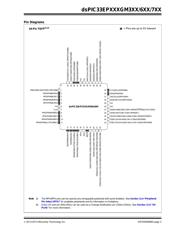
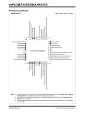
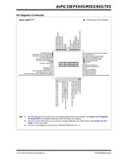
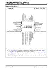
引脚图在P3P4P5P6P7P8P16P17P18P19P22P164Hot
典型应用电路图在P24
原理图在P15P28P111P131P144P163P211P214P215P219P223P258
封装尺寸在P509
标记信息在P507P508
封装信息在P434P507P510P514P515P516P517P518P519P521P523P524
功能描述在P219P327P395
技术参数、封装参数在P326P435P440P441P442P443P445P447P488P489P490P491
电气规格在P22P173P273P275P326P329P368P369P416P443
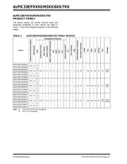
型号编号列表在P2P104
导航目录
DSPIC33EP512GM710-I/PT数据手册
Page:
of 542 Go
若手册格式错乱,请下载阅览PDF原文件

2013-2014 Microchip Technology Inc. DS70000689D-page 1
dsPIC33EPXXXGM3XX/6XX/7XX
Operating Conditions
• 3.0V to 3.6V, -40°C to +85°C, up to 70 MIPS
• 3.0V to 3.6V, -40°C to +125°C, up to 60 MIPS
Core: 16-Bit dsPIC33E CPU
• Code-Efficient (C and Assembly) Architecture
• Two 40-Bit Wide Accumulators
• Single-Cycle (MAC/MPY) with Dual Data Fetch
• Single-Cycle Mixed-Sign MUL plus Hardware Divide
• 32-Bit Multiply Support
Clock Management
• Internal Fast FRC Oscillator with 1% Accuracy
• Programmable PLLs and Oscillator Clock Sources
• Fail-Safe Clock Monitor (FSCM)
• Independent Watchdog Timer (WDT)
• Fast Wake-up and Start-up
Power Management
• Low-Power Management modes (Sleep, Idle, Doze)
• Executing Optimized NOP String with Flash Fetch
• Integrated Power-on Reset and Brown-out Reset
• 0.6 mA/MHz Dynamic Current (typical)
•30 µA IPD Current (typical)
High-Speed PWM
• Up to 12 PWM Outputs (six generators)
• Primary Master Time Base Inputs allow Time Base
Synchronization from Internal/External Sources
• Dead Time for Rising and Falling Edges
• 7.14 ns PWM Resolution
• PWM Support for:
- DC/DC, AC/DC, Inverters, PFC, Lighting
- BLDC, PMSM, ACIM, SRM
• Programmable Fault Inputs
• Flexible Trigger Configurations for ADC Conversions
• Supports PWM Lock, PWM Output Chopping and
Dynamic Phase Shifting
Advanced Analog Features
• Two Independent ADC modules:
- Configurable as 10-bit, 1.1 Msps with
four S&H or 12-bit, 500 ksps with one S&H
- 11, 13, 18, 30 or 49 analog inputs
• Flexible and Independent ADC Trigger Sources
• Up to Four Op Amp/Comparators with Direct
Connection to the ADC module:
- Additional dedicated comparator
- Programmable references with 32 voltage points
- Programmable blanking and filtering
• Charge Time Measurement Unit (CTMU):
- Supports mTouch™ capacitive touch sensing
- Provides high-resolution time measurement (1 ns)
- On-chip temperature measurement
Timers/Output Compare/Input Capture
• 21 General Purpose Timers:
- Nine 16-bit and up to four 32-bit timers/counters
- Eight output capture modules configurable as
timers/counters
- PTG module with two configurable timers/counters
- Two 32-bit Quadrature Encoder Interface (QEI)
modules configurable as a timer/counter
• Eight Input Capture modules
• Peripheral Pin Select (PPS) to allow Function Remap
• Peripheral Trigger Generator (PTG) for Scheduling
Complex Sequences
Communication Interfaces
• Four Enhanced Addressable UART modules
(17.5 Mbps):
- With support for LIN/J2602 protocols and IrDA
®
• Three 3-Wire/4-Wire SPI modules (15 Mbps)
• 25 Mbps Data Rate for Dedicated SPI module
(with no PPS)
•Two I
2
C™ modules (up to 1 Mbps) with SMBus Support
• Two CAN modules (1 Mbps) with CAN 2.0B Support
• Programmable Cyclic Redundancy Check (CRC)
• Codec Interface module (DCI) with I
2
S Support
Direct Memory Access (DMA)
• 4-Channel DMA with User-Selectable Priority Arbitration
• Peripherals Supported by the DMA Controller include:
- UART, SPI, ADC, CAN and input capture
- Output compare and timers
Input/Output
• Sink/Source 15 mA or 10 mA, Pin-Specific for
Standard V
OH/VOL
• 5V Tolerant Pins
• Selectable Open-Drain, Pull-ups and Pull-Downs
• Up to 5 mA Overvoltage Clamp Current
• Change Notice Interrupts on All I/O Pins
• PPS to allow Function Remap
Qualification and Class B Support
• AEC-Q100 REVG (Grade 1, -40°C to +125°C) Planned
• AEC-Q100 REVG (Grade 0, -40°C to +150°C) Planned
• Class B Safety Library, IEC 60730
Debugger Development Support
• In-Circuit and In-Application Programming
• Three Complex and Five Simple Breakpoints
• IEEE 1149.2 Compatible (JTAG) Boundary Scan
• Trace and Run-Time Watch
16-Bit Digital Signal Controllers with High-Speed PWM,
Op Amps and Advanced Analog Features
器件 Datasheet 文档搜索
AiEMA 数据库涵盖高达 72,405,303 个元件的数据手册,每天更新 5,000 多个 PDF 文件
