Datasheet 搜索 > 双极性晶体管 > ON Semiconductor(安森美) > DTA144EET1 数据手册 > DTA144EET1 产品封装文件 1/13 页
 器件3D模型
¥ 0.288
DTA144EET1 产品封装文件 - ON Semiconductor(安森美)
制造商:
ON Semiconductor(安森美)
分类:
双极性晶体管
封装:
SC-75-3
描述:
DTA144EET1 带阻尼PNP三极管 -50V -30mA 0.15W/150mW SOT-523/SC-75 标记6C 开关电路,逆变器,接口电路,驱动电路
Pictures:
3D模型
符号图
焊盘图
引脚图
产品图
页面导航:
典型应用电路图在P10
封装尺寸在P13
焊盘布局在P13
型号编码规则在P1P4P13
标记信息在P1P4
封装信息在P4
技术参数、封装参数在P4
应用领域在P1
电气规格在P2P3P6P7P8P9P10P11P12
导航目录
DTA144EET1数据手册
Page:
of 13 Go
若手册格式错乱,请下载阅览PDF原文件
Semiconductor Components Industries, LLC, 2011
November, 2011 − Rev. 7
1 Publication Order Number:
DTA114EET1/D
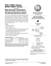
DTA114EET1 Series,
SDTA114EET1 Series
Preferred Devices
Bias Resistor Transistors
PNP Silicon Surface Mount Transistors
with Monolithic Bias Resistor Network
This new series of digital transistors is designed to replace a single
device and its external resistor bias network. The Bias Resistor
Transistor (BRT) contains a single transistor with a monolithic bias
network consisting of two resistors; a series base resistor and a
base−emitter resistor. The BRT eliminates these individual
components by integrating them into a single device. The use of a BRT
can reduce both system cost and board space. The device is housed in
the SC−75/SOT−416 package which is designed for low power
surface mount applications.
Features
Simplifies Circuit Design
Reduces Board Space
Reduces Component Count
The SC−75/SOT−416 package can be soldered using wave or reflow.
The modified gull−winged leads absorb thermal stress during
soldering eliminating the possibility of damage to the die.
AEC−Q101 Qualified and PPAP Capable
S Prefix for Automotive and Other Applications Requiring Unique
Site and Control Change Requirements
Pb−Free Packages are Available*
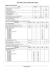
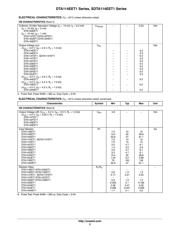
MAXIMUM RATINGS (T
A
= 25C unless otherwise noted)
Rating
Symbol Value Unit
Collector-Base Voltage V
CBO
50 Vdc
Collector-Emitter Voltage V
CEO
50 Vdc
Collector Current I
C
100 mAdc
Stresses exceeding Maximum Ratings may damage the device. Maximum
Ratings are stress ratings only. Functional operation above the Recommended
Operating Conditions is not implied. Extended exposure to stresses above the
Recommended Operating Conditions may affect device reliability.
*For additional information on our Pb−Free strategy and soldering details, please
download the ON Semiconductor Soldering and Mounting Techniques
Reference Manual, SOLDERRM/D.
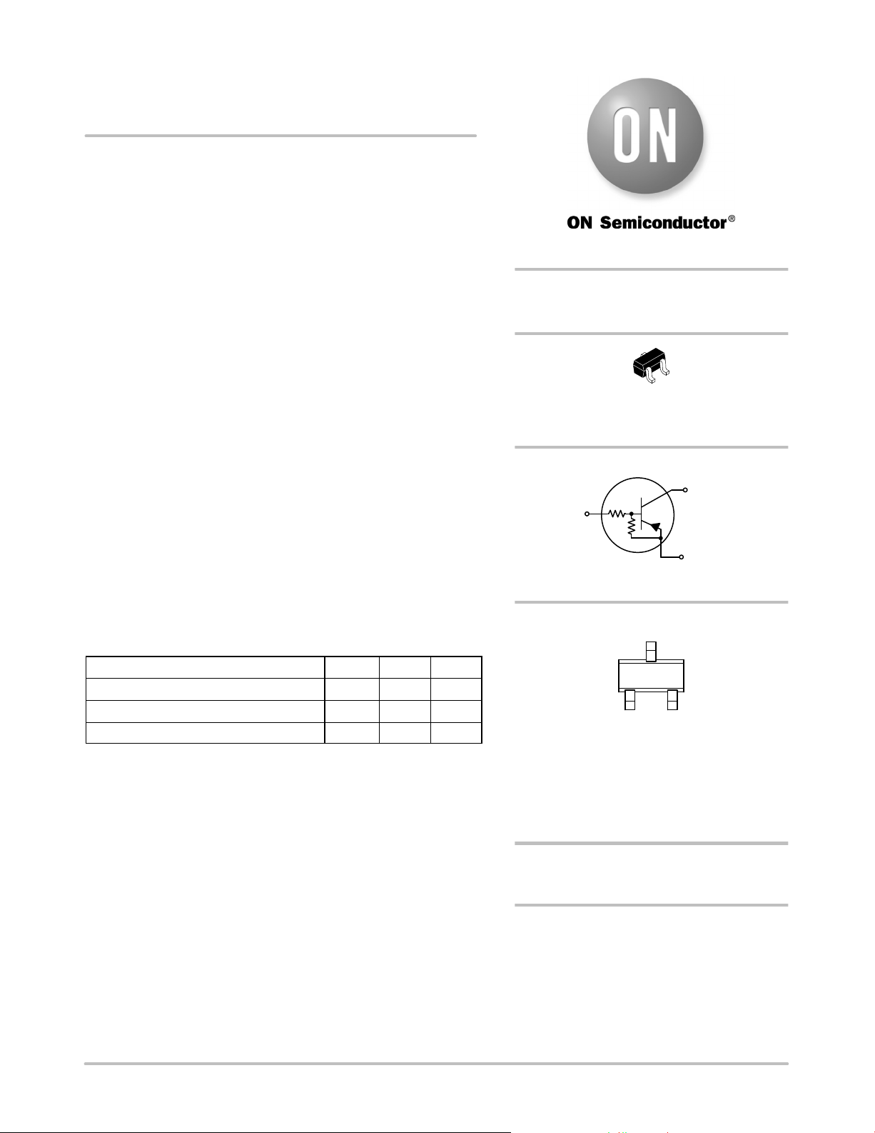
SC−75 (SOT−416)
CASE 463
STYLE 1
Preferred devices are recommended choices for future use
and best overall value.
PNP SILICON BIAS
RESISTOR TRANSISTORS
PIN 3
COLLECTOR
(OUTPUT)
PIN 2
EMITTER
(GROUND)
PIN 1
BASE
(INPUT)
R1
R2
MARKING DIAGRAM
xx M G
G
http://onsemi.com
See detailed ordering and shipping information in the package
dimensions section on page 4 of this data sheet.
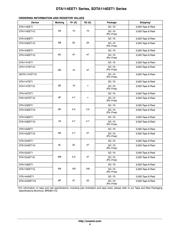
ORDERING INFORMATION
xx = Specific Device Code
xx = (Refer to page 4)
M = Date Code*
G =Pb−Free Package
(Note: Microdot may be in either location)
*Date Code orientation may vary depending
upon manufacturing location.
器件 Datasheet 文档搜索
AiEMA 数据库涵盖高达 72,405,303 个元件的数据手册,每天更新 5,000 多个 PDF 文件
