Datasheet 搜索 > FPGA芯片 > Altera(阿尔特拉) > EP3C40F324A7N 数据手册 > EP3C40F324A7N 其他数据使用手册 1/12 页

 器件3D模型
¥ 300.518
EP3C40F324A7N 其他数据使用手册 - Altera(阿尔特拉)
制造商:
Altera(阿尔特拉)
分类:
FPGA芯片
封装:
FBGA-324
Pictures:
3D模型
符号图
焊盘图
引脚图
产品图
页面导航:
导航目录
EP3C40F324A7N数据手册
Page:
of 12 Go
若手册格式错乱,请下载阅览PDF原文件
SCLS564A − JANUARY 2004 − REVISED MAY 2004
1
POST OFFICE BOX 655303 • DALLAS, TEXAS 75265
D Controlled Baseline
− One Assembly/Test Site, One Fabrication
Site
D Extended Temperature Performance of
−40°C to 105°C
D Enhanced Diminishing Manufacturing
Sources (DMS) Support
D Enhanced Product-Change Notification
D Qualification Pedigree
†
D 2-V to 5.5-V V
CC
Operation
†
Component qualification in accordance with JEDEC and industry
standards to ensure reliable operation over an extended
temperature range. This includes, but is not limited to, Highly
Accelerated Stress Test (HAST) or biased 85/85, temperature
cycle, autoclave or unbiased HAST, electromigration, bond
intermetallic life, and mold compound life. Such qualification
testing should not be viewed as justifying use of this component
beyond specified performance and environmental limits.
D Typical V
OLP
(Output Ground Bounce)
<0.8 V at V
CC
= 3.3 V, T
A
= 25°C
D Typical V
OHV
(Output V
OH
Undershoot)
>2.3 V at V
CC
= 3.3 V, T
A
= 25°C
D Supports Mixed-Mode Voltage Operation on
All Ports
D I
off
Supports Partial-Power-Down Mode
Operation
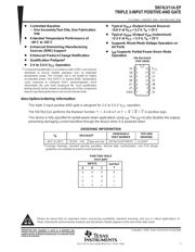
description/ordering information
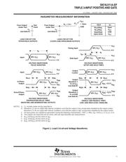
This triple 3-input positive-AND gate is designed for 2-V to 5.5-V V
CC
operation.
The SN74LV11A performs the Boolean function
Y + A • B • CorY+ A
) B ) C
in positive logic.
This device is fully specified for partial-power-down applications using I
off
. The I
off
circuitry disables the outputs,
preventing damaging current backflow through the device when it is powered down.
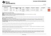
ORDERING INFORMATION
T
A
PACKAGE
‡
ORDERABLE
PART NUMBER
TOP-SIDE
MARKING
−40°C to 105°C TSSOP − PW Tape and reel SN74LV11ATPWREP LV11AEP
‡
Package drawings, standard packing quantities, thermal data, symbolization, and PCB design
guidelines are available at www.ti.com/sc/package.
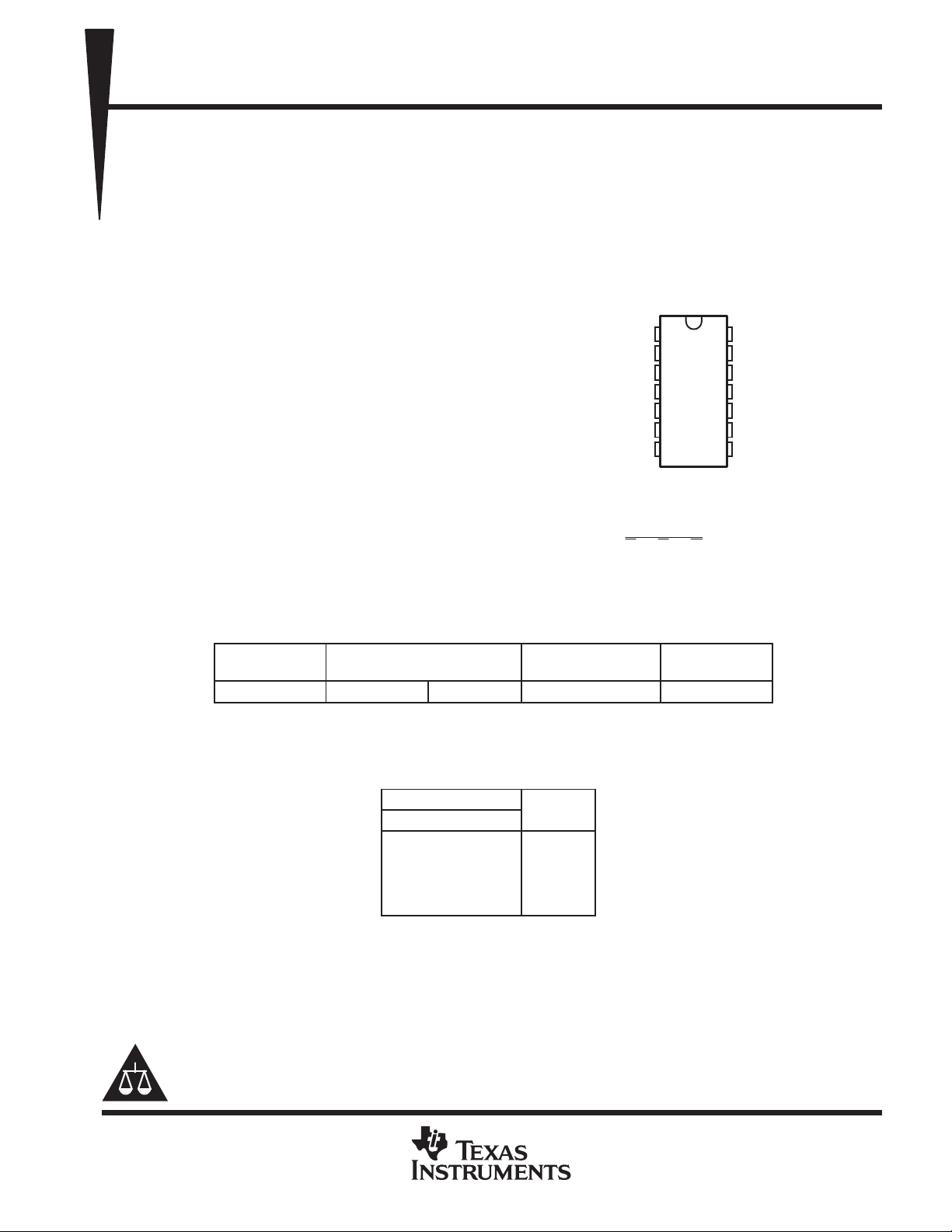
FUNCTION TABLE
(each gate)
INPUTS
OUTPUT
A B C
OUTPUT
Y
H H H H
L XX L
X LX L
X X L L
Copyright 2004, Texas Instruments Incorporated
PW PACKAGE
(TOP VIEW)
1
2
3
4
5
6
7
14
13
12
11
10
9
8
1A
1B
2A
2B
2C
2Y
GND
V
CC
1C
1Y
3C
3B
3A
3Y
Please be aware that an important notice concerning availability, standard warranty, and use in critical applications of
Texas Instruments semiconductor products and disclaimers thereto appears at the end of this data sheet.
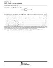
! "#$ %!&
% "! "! '! ! !( !
%% )*& % "!+ %! !!$* $%!
!+ $$ "!!&
器件 Datasheet 文档搜索
AiEMA 数据库涵盖高达 72,405,303 个元件的数据手册,每天更新 5,000 多个 PDF 文件
