Datasheet 搜索 > 负载控制器 > Fairchild(飞兆/仙童) > FDC6331L 数据手册 > FDC6331L 其他数据使用手册 1/5 页
 器件3D模型
¥ 1.933
FDC6331L 其他数据使用手册 - Fairchild(飞兆/仙童)
制造商:
Fairchild(飞兆/仙童)
分类:
负载控制器
封装:
TSOT-23-6
描述:
FAIRCHILD SEMICONDUCTOR FDC6331L 集成负载开关, 高压侧, 高电平有效, 1路输出, 8V, 2.8A, SSOT-6
Pictures:
3D模型
符号图
焊盘图
引脚图
产品图
页面导航:
导航目录
FDC6331L数据手册
Page:
of 5 Go
若手册格式错乱,请下载阅览PDF原文件
August 2001
2007 Fairchild Semiconductor Corporation FDC6331L Rev D
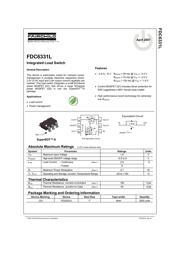
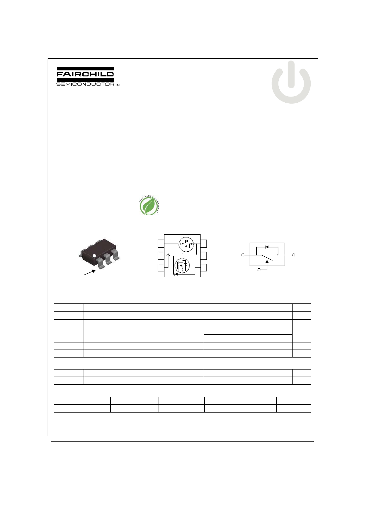
FDC6331L
Integrated Load Switch
General Description
This device is particularly suited for compact power
management in portable electronic equipment where
2.5V to 8V input and 2.8A output current capability are
needed. This load switch integrates a small N-Channel
power MOSFET (Q1) that drives a large P-Channel
power MOSFET (Q2) in one tiny SuperSOT
TM
-6
package.
Applications
x Load switch
x Power management
Features
x –2.8 A, –8 V. R
DS(ON)
= 55 m: @ V
GS
= –4.5 V
R
DS(ON)
= 70 m: @ V
GS
= –2.5 V
R
DS(ON)
= 100 m:@ V
GS
= –1.8 V
x Control MOSFET (Q1) includes Zener protection for
ESD ruggedness (>6KV Human body model)
x High performance trench technology for extremely
low R
DS(ON)
D1
S2
G1
D2
S1
G2
SuperSOT -6
TM
Pin 1
SuperSOT™-6
3
2
1
4
5
6
Q1
Q2
Vout,C1
Vout,C1
R2
Vin,R1
ON/O FF
R1,C1
See Application Circuit
Equivalent Circuit
V
DR O P
+–
IN OUT
ON/OFF
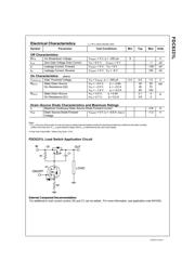
Absolute Maximum Ratings T
A
=25
o
C unless otherwise noted
Symbol Parameter Ratings Units
V
IN
Maximum Input Voltage r 8V
V
ON/OFF
High level ON/OFF voltage range –0.5 to 8 V
I
Load
Load Current – Continuous (Note 1) 2.8 A
– Pulsed 9
P
D
Maximum Power Dissipation (Note 1) 0.7 W
T
J
, T
STG
Operating and Storage Junction Temperature Range –55 to +150 qC
Thermal Characteristics
R
TJA
Thermal Resistance, Junction-to-Ambient (Note 1) 180
qC/W
R
TJC
Thermal Resistance, Junction-to-Case (Note 1) 60
qC/W
Package Marking and Ordering Information
Device Marking Device Reel Size Tape width Quantity
.331 FDC6331L 7’’ 8mm 3000 units
FDC6331L
tm
April 2007
器件 Datasheet 文档搜索
AiEMA 数据库涵盖高达 72,405,303 个元件的数据手册,每天更新 5,000 多个 PDF 文件
