Datasheet 搜索 > MOS管 > Fairchild(飞兆/仙童) > FDG6306P 数据手册 > FDG6306P 其他数据使用手册 3/7 页

 器件3D模型
¥ 7.589
FDG6306P 其他数据使用手册 - Fairchild(飞兆/仙童)
制造商:
Fairchild(飞兆/仙童)
分类:
MOS管
封装:
SC-70-6
描述:
FAIRCHILD SEMICONDUCTOR FDG6306P 双路场效应管, MOSFET, 双P沟道, -600 mA, -20 V, 0.3 ohm, -4.5 V, -1.2 V
Pictures:
3D模型
符号图
焊盘图
引脚图
产品图
页面导航:


导航目录
FDG6306P数据手册
Page:
of 7 Go
若手册格式错乱,请下载阅览PDF原文件
FDG6306P Rev 1.3
(W)
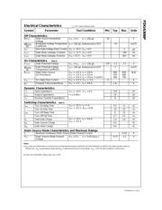
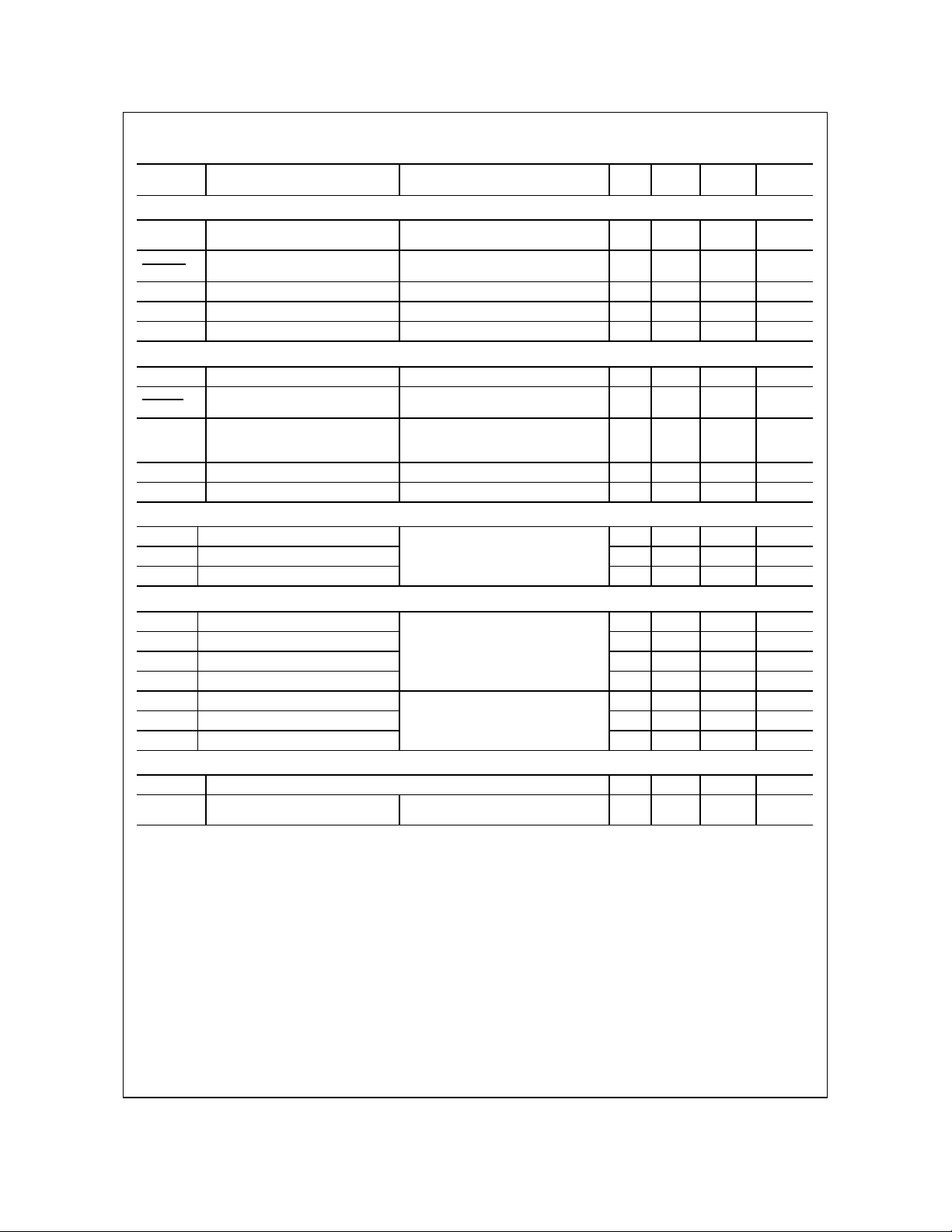
Electrical Characteristics T
A
= 25°C unless otherwise noted
Symbol Parameter Test Conditions Min Typ Max Units
Off Characteristics
BV
DSS
Drain–Source Breakdown
Voltage
V
GS
= 0 V, I
D
= –250 µA
–20 V
∆BVDSS
∆T
J
Breakdown Voltage Temperature
Coefficient
I
D
= –250 µA, Referenced to 25°C
–14
mV/°C
I
DSS
Zero Gate Voltage Drain Current V
DS
= –16 V, V
GS
= 0 V –1
µA
I
GSSF
Gate–Body Leakage, Forward V
GS
= –12 V, V
DS
= 0 V –100 nA
I
GSSR
Gate–Body Leakage, Reverse V
GS
= 12 V, V
DS
= 0 V 100 nA
On Characteristics (Note 2)
V
GS(th)
Gate Threshold Voltage
V
DS
= V
GS
, I
D
= –250 µA
–0.6 –1.2 –1.5 V
∆VGS(th)
∆T
J
Gate Threshold Voltage
Temperature Coefficient
I
D
= –250 µA, Referenced to 25°C
3
mV/°C
R
DS(on)
Static Drain–Source
On–Resistance
V
GS
= –4.5 V, I
D
= –0.6 A
V
GS
= –2.5 V, I
D
= –0.5 A
V
GS
= –4.5 V, I
D
= –0.6 A, T
J
=125°C
300
470
400
420
630
700
M Ω
I
D(on)
On–State Drain Current V
GS
= –4.5 V, V
DS
= –5 V –2 A
g
FS
Forward Transconductance V
DS
= –5 V, I
D
= –0.6 A 1.8 S
Dynamic Characteristics
C
iss
Input Capacitance 114 pF
C
oss
Output Capacitance 24 pF
C
rss
Reverse Transfer Capacitance
V
DS
= –10 V, V
GS
= 0 V,
f = 1.0 MHz
9 pF
Switching Characteristics (Note 2)
t
d(on)
Turn–On Delay Time 5.5 11 ns
t
r
Turn–On Rise Time 14 25 ns
t
d(off)
Turn–Off Delay Time 6 12 ns
t
f
Turn–Off Fall Time
V
DD
= –10 V, I
D
= 1 A,
V
GS
= –4.5 V, R
GEN
= 6 Ω
1.7 3.4 ns
Q
g
Total Gate Charge 1.4 2.0 nC
Q
gs
Gate–Source Charge 0.3 nC
Q
gd
Gate–Drain Charge
V
DS
= –10 V, I
D
= –0.6 A,
V
GS
= –4.5 V
0.4 nC
Drain–Source Diode Characteristics and Maximum Ratings
I
S
Maximum Continuous Drain–Source Diode Forward Current –0.25 A
V
SD
Drain–Source Diode Forward
Voltage
V
GS
= 0 V, I
S
= –0.25 A(Note 2) –0.77 –1.2 V
Notes:
1. R
θJA
is the sum of the junction-to-case and case-to-ambient thermal resistance where the case thermal reference is defined as the solder mounting surface of
the drain pins. R
θJC
is guaranteed by design while R
θJA
is determined by the user's board design. R
θJA
= 415°C/W when mounted on a minimum pad .
2. Pulse Test: Pulse Width < 300µs, Duty Cycle < 2.0%
FDG6306P
器件 Datasheet 文档搜索
AiEMA 数据库涵盖高达 72,405,303 个元件的数据手册,每天更新 5,000 多个 PDF 文件
