Datasheet 搜索 > ON Semiconductor(安森美) > FDS6690 数据手册 > FDS6690 其他数据使用手册 1/6 页


¥ 0
FDS6690 其他数据使用手册 - ON Semiconductor(安森美)
制造商:
ON Semiconductor(安森美)
封装:
751EB
Pictures:
3D模型
符号图
焊盘图
引脚图
产品图
页面导航:
导航目录
FDS6690数据手册
Page:
of 6 Go
若手册格式错乱,请下载阅览PDF原文件
Publication Order Number:
FDS6690A/D
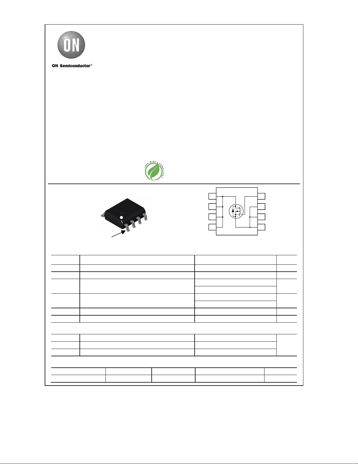
FDS6690A
Single N-Channel, Logic-Level, PowerTrench
MOSFET
General Description
This N-Channel Logic Level MOSFET is
produced using ON Semiconductor’s
advanced PowerTrench process that has been
especially tailored to minimize the on-state resistance
and yet maintain superior switching performance.
These devices are well suited for low voltage
and battery powered applications where low in-line
power loss and fast switching are required.
Features
• 11 A, 30 V. R
DS(ON)
= 12.5 mΩ @ V
GS
= 10 V
R
DS(ON)
= 17.0 mΩ @ V
GS
= 4.5 V
• Fast switching speed
• Low gate charge
• High performance trench technology for extremely
low R
DS(ON)
• High power and current handling capability
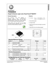
S
D
S
S
SO-8
D
D
D
G
D
D
D
D
S
S
S
G
Pin 1
SO-8
4
3
2
1
5
6
7
8
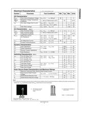
Absolute Maximum Ratings T
A
=25
o
C unless otherwise noted
Symbol Parameter Ratings Units
V
DSS
Drain-Source Voltage 30 V
V
GSS
Gate-Source Voltage
±20
V
I
D
Drain Current – Continuous
(Note 1a)
11 A
– Pulsed 50
Power Dissipation for Single Operation
(Note 1a)
2.5
P
D
(Note 1b)
1.0
W
E
AS
Single Pulse Avalanche Energy
(Note 3)
96 mJ
T
J
, T
STG
Operating and Storage Junction Temperature Range –55 to +150
°C
Thermal Characteristics
R
θJA
Thermal Resistance, Junction-to-Ambient
(Note 1a)
50
°C/W
R
θJA
Thermal Resistance, Junction-to-Ambient
(Note 1b)
125
R
θJC
Thermal Resistance, Junction-to-Case
(Note 1)
25
Package Marking and Ordering Information
Device Marking Device Reel Size Tape width Quantity
FDS6690A FDS6690A 13’’ 12mm 2500 units
FDS6
690A
© 2007 Semiconductor Components Industries, LLC.
October-2017, Rev. 5
器件 Datasheet 文档搜索
AiEMA 数据库涵盖高达 72,405,303 个元件的数据手册,每天更新 5,000 多个 PDF 文件
