Datasheet 搜索 > Fairchild(飞兆/仙童) > H11AA4SR2V-M 数据手册 > H11AA4SR2V-M 其他数据使用手册 4/10 页


¥ 0
H11AA4SR2V-M 其他数据使用手册 - Fairchild(飞兆/仙童)
制造商:
Fairchild(飞兆/仙童)
Pictures:
3D模型
符号图
焊盘图
引脚图
产品图
页面导航:
导航目录
H11AA4SR2V-M数据手册
Page:
of 10 Go
若手册格式错乱,请下载阅览PDF原文件
©2006 Fairchild Semiconductor Corporation www.fairchildsemi.com
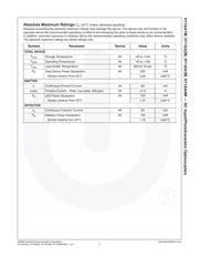
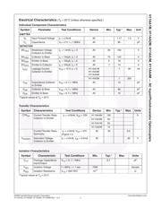
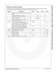
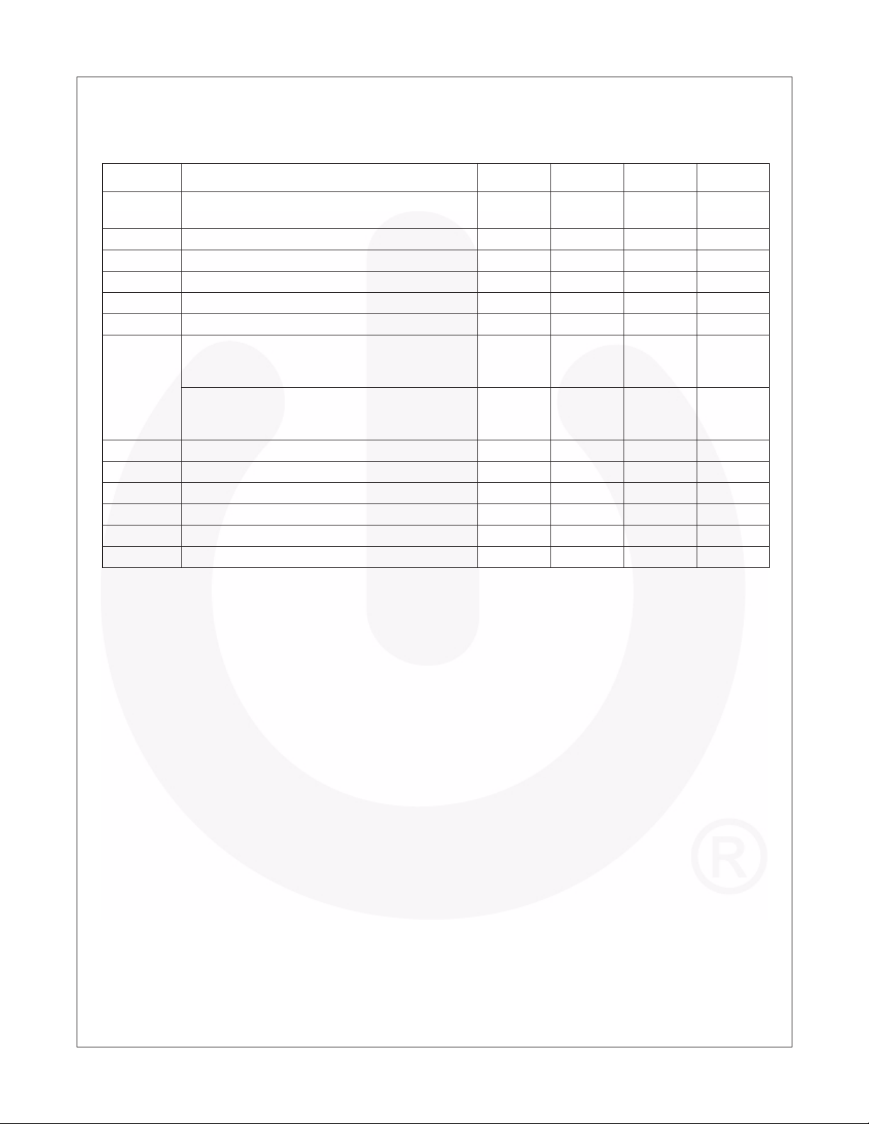
H11AA1M, H11AA2M, H11AA3M, H11AA4M Rev. 1.0.3 4
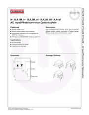
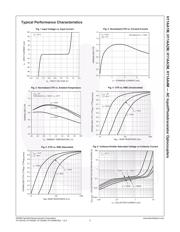
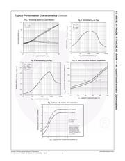
H11AA1M, H11AA2M, H11AA3M, H11AA4M — AC Input/Phototransistor Optocouplers
Safety and Insulation Ratings
As per IEC 60747-5-2, this optocoupler is suitable for “safe electrical insulation” only within the safety limit data.
Compliance with the safety ratings shall be ensured by means of protective circuits.
Symbol Parameter Min. Typ. Max. Unit
Installation Classifications per DIN VDE 0110/1.89
Table 1
For Rated Main Voltage < 150Vrms I-IV
For Rated Main voltage < 300Vrms I-IV
Climatic Classification 55/100/21
Pollution Degree (DIN VDE 0110/1.89) 2
CTI Comparative Tracking Index 175
V
PR
Input to Output Test Voltage, Method b,
V
IORM
x 1.875 = V
PR
, 100% Production Test
with tm = 1 sec, Partial Discharge < 5pC
1594 V
peak
Input to Output Test Voltage, Method a,
V
IORM
x 1.5 = V
PR
, Type and Sample Test
with tm = 60 sec, Partial Discharge < 5pC
1275 V
peak
V
IORM
Max. Working Insulation Voltage 850 V
peak
V
IOTM
Highest Allowable Over Voltage 6000 V
peak
External Creepage 7 mm
External Clearance 7 mm
Insulation Thickness 0.5 mm
RIO Insulation Resistance at Ts, V
IO
= 500V 10
9
Ω
器件 Datasheet 文档搜索
AiEMA 数据库涵盖高达 72,405,303 个元件的数据手册,每天更新 5,000 多个 PDF 文件
