Datasheet 搜索 > 光耦合器/光隔离器 > Fairchild(飞兆/仙童) > H11G2M 数据手册 > H11G2M 其他数据使用手册 3/12 页
 器件3D模型
¥ 1.769
H11G2M 其他数据使用手册 - Fairchild(飞兆/仙童)
制造商:
Fairchild(飞兆/仙童)
分类:
光耦合器/光隔离器
封装:
DIP-6
描述:
FAIRCHILD SEMICONDUCTOR H11G2M 光电耦合器, 光敏达林顿, 7.5KV, DIP
Pictures:
3D模型
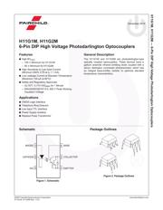
符号图
焊盘图
引脚图
产品图

H11G2M数据手册
Page:
of 12 Go
若手册格式错乱,请下载阅览PDF原文件
©2007 Fairchild Semiconductor Corporation www.fairchildsemi.com
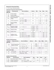
H11G1M, H11G2M Rev. 1.0.5 2
H11G1M, H11G2M — 6-Pin DIP High Voltage Photodarlington Optocouplers
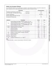
Safety and Insulation Ratings
As per DIN EN/IEC 60747-5-5, this optocoupler is suitable for “safe electrical insulation” only within the safety limit
data. Compliance with the safety ratings shall be ensured by means of protective circuits.
Note:
1. Safety limit values – maximum values allowed in the event of a failure.
Parameter Characteristics
Installation Classifications per DIN VDE
0110/1.89 Table 1, For Rated Mains Voltage
< 150 V
RMS
I–IV
< 300 V
RMS
I–IV
Climatic Classification 55/100/21
Pollution Degree (DIN VDE 0110/1.89) 2
Comparative Tracking Index 175
Symbol Parameter Value Unit
V
PR
Input-to-Output Test Voltage, Method A, V
IORM
x 1.6 = V
PR
,
Type and Sample Test with t
m
= 10 s, Partial Discharge < 5 pC
1360 V
peak
Input-to-Output Test Voltage, Method B, V
IORM
x 1.875 = V
PR
,
100% Production Test with t
m
= 1 s, Partial Discharge < 5 pC
1594 V
peak
V
IORM
Maximum Working Insulation Voltage 850 V
peak
V
IOTM
Highest Allowable Over-Voltage 6000 V
peak
External Creepage
≥
7mm
External Clearance
≥
7mm
External Clearance (for Option TV, 0.4" Lead Spacing)
≥
10 mm
DTI Distance Through Insulation (Insulation Thickness)
≥
0.5 mm
T
S
Case Temperature
(1)
175 °C
I
S,INPUT
Input Current
(1)
350 mA
P
S,OUTPUT
Output Power
(1)
800 mW
R
IO
Insulation Resistance at T
S
, V
IO
= 500 V
(1)
> 10
9
Ω
器件 Datasheet 文档搜索
AiEMA 数据库涵盖高达 72,405,303 个元件的数据手册,每天更新 5,000 多个 PDF 文件
