Datasheet 搜索 > Hittite > HMC1118LP3DETR 数据手册 > HMC1118LP3DETR 其他数据使用手册 1/12 页

¥ 79.418
HMC1118LP3DETR 其他数据使用手册 - Hittite
制造商:
Hittite
封装:
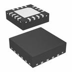
VFQFN-16
Pictures:
3D模型
符号图
焊盘图
引脚图
产品图
页面导航:
导航目录
HMC1118LP3DETR数据手册
Page:
of 12 Go
若手册格式错乱,请下载阅览PDF原文件
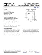
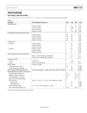
High Isolation, Silicon SPDT,
Nonrefective Switch, 9 kHz to 13.0 GHz
Data Sheet
HMC1118
Rev. 0 Document Feedback
Information furnished by Analog Devices is believed to be accurate and reliable. However, no
responsibility is assumed by Analog Devices for its use, nor for any infringements of patents or other
rights of third parties that may result from its use. Specifications subject to change without notice. No
license is granted by implication or otherwise under any patent or patent rights of Analog Devices.
Trademarks and registered trademarks are the property of their respective owners.
One Technology Way, P.O. Box 9106, Norwood, MA 02062-9106, U.S.A.
Tel: 781.329.4700 ©2015 Analog Devices, Inc. All rights reserved.
Technical Support www.analog.com
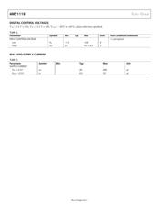
FEATURES
Nonreflective 50 Ω design
Positive control: 0 V/3.3 V
Low insertion loss: 0.68 dB at 8.0 GHz
High isolation: 48 dB at 8.0 GHz
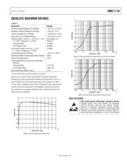
High power handling
35 dBm through path
27 dBm terminated path
High linearity
1 dB compression (P1dB): 37 dBm typical
Input third-order intercept (IIP3): 62 dBm typical
ESD rating: 2 kV human body model (HBM)
3 mm × 3 mm, 16-lead LFCSP package
No low frequency spurious
Settling time (0.05 dB margin of final RF
OUT
): 7.5 µs
APPLICATIONS
Test instrumentation
Microwave radios and very small aperture terminals (VSATs)
Military radios, radars, and electronic counter measures (ECMs)
Fiber optics and broadband telecommunications
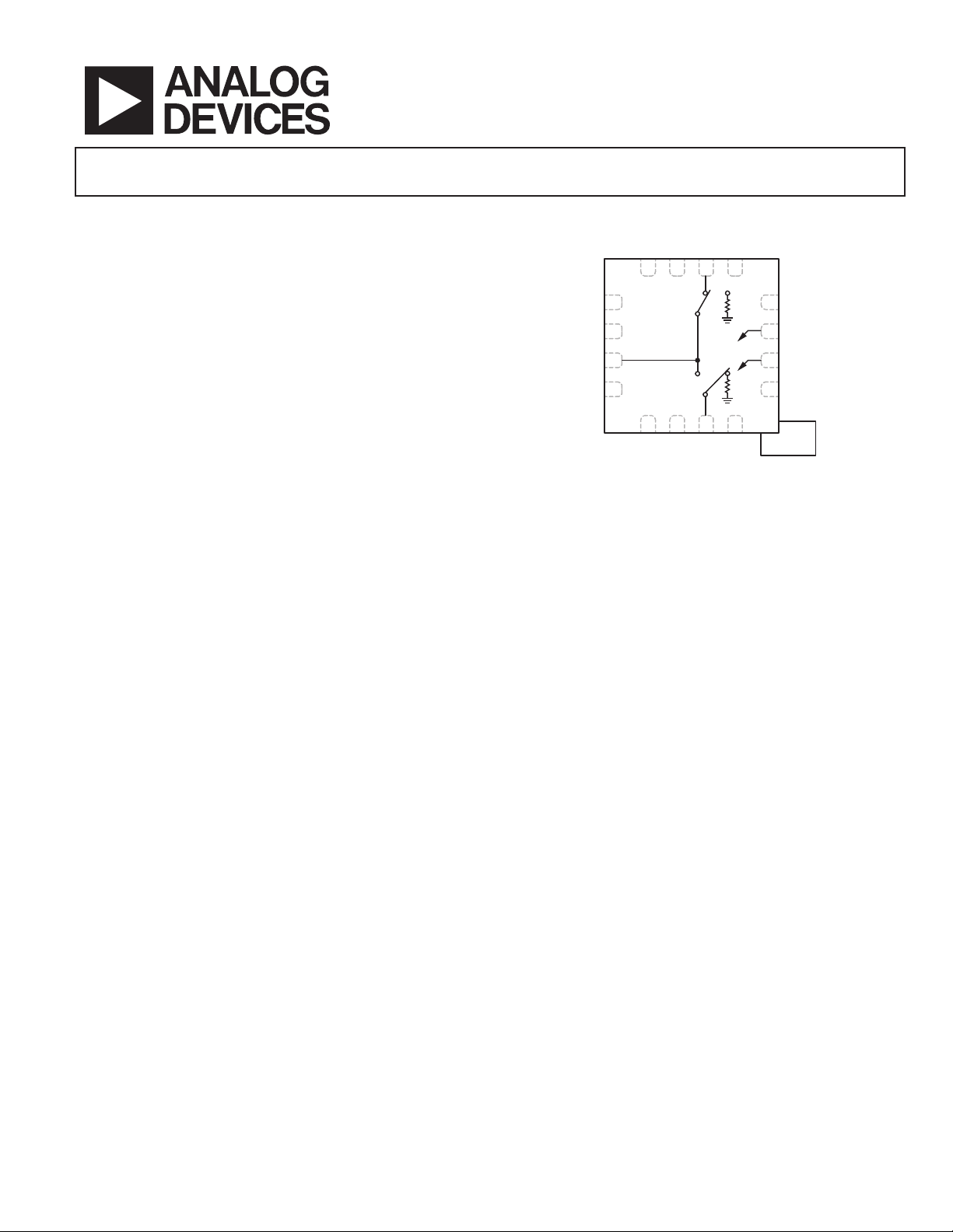
FUNCTIONAL BLOCK DIAGRAM
1
2
3
4
GND
GND
RFC
GND
12
11
10
9
V
DD
LS
V
CTRL
V
SS
5
6
7
8
GND
GND
RF2
GND
16
15
14
13
GND
GND
RF1
GND
ȍ
ȍ
PACKAGE
BASE
GND
HMC1118
12961-001
Figure 1.
GENERAL DESCRIPTION
The HMC1118 is a general-purpose, broadband, nonreflective
single-pole, double-throw (SPDT) switch in a LFCSP surface
mount package. Covering the 9 kHz to 13.0 GHz range, the
switch offers high isolation and low insertion loss. The switch
features >48 dB isolation, 0.68 dB insertion loss up to 8.0 GHz,
and a 7.5 µs settling time of 0.05 dB margin of final RF
OUT
. The
switch operates using positive control voltage logic lines of +3.3 V
and 0 V and requires +3.3 V and −2.5 V supplies. The
HMC1118
can cover the same operating frequency range with a single
positive supply voltage applied and the negative supply voltage
(V
SS
) tied to ground and still maintaining good power handling
performance. The
HMC1118 is packaged in a 3 mm × 3 mm,
surface mount LFCSP package.
器件 Datasheet 文档搜索
AiEMA 数据库涵盖高达 72,405,303 个元件的数据手册,每天更新 5,000 多个 PDF 文件
