Datasheet 搜索 > MOS管 > Vishay Siliconix > IRFPC50 数据手册 > IRFPC50 其他数据使用手册 2/9 页

¥ 0
IRFPC50 其他数据使用手册 - Vishay Siliconix
制造商:
Vishay Siliconix
分类:
MOS管
封装:
TO-247-3
Pictures:
3D模型
符号图
焊盘图
引脚图
产品图
页面导航:
封装尺寸在P8
型号编码规则在P1
功能描述在P1P9
技术参数、封装参数在P1P2P9
导航目录
IRFPC50数据手册
Page:
of 9 Go
若手册格式错乱,请下载阅览PDF原文件
www.vishay.com Document Number: 91243
2 S11-0443-Rev. B, 14-Mar-11
This datasheet is subject to change without notice.
THE PRODUCT DESCRIBED HEREIN AND THIS DATASHEET ARE SUBJECT TO SPECIFIC DISCLAIMERS, SET FORTH AT
www.vishay.com/doc?91000
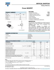
IRFPC50, SiHFPC50
Vishay Siliconix
Notes
a. Repetitive rating; pulse width limited by maximum junction temperature (see fig. 11).
b. Pulse width ≤ 300 μs; duty cycle ≤ 2 %.
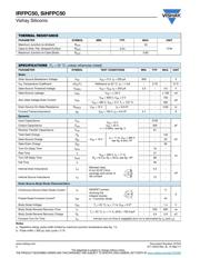
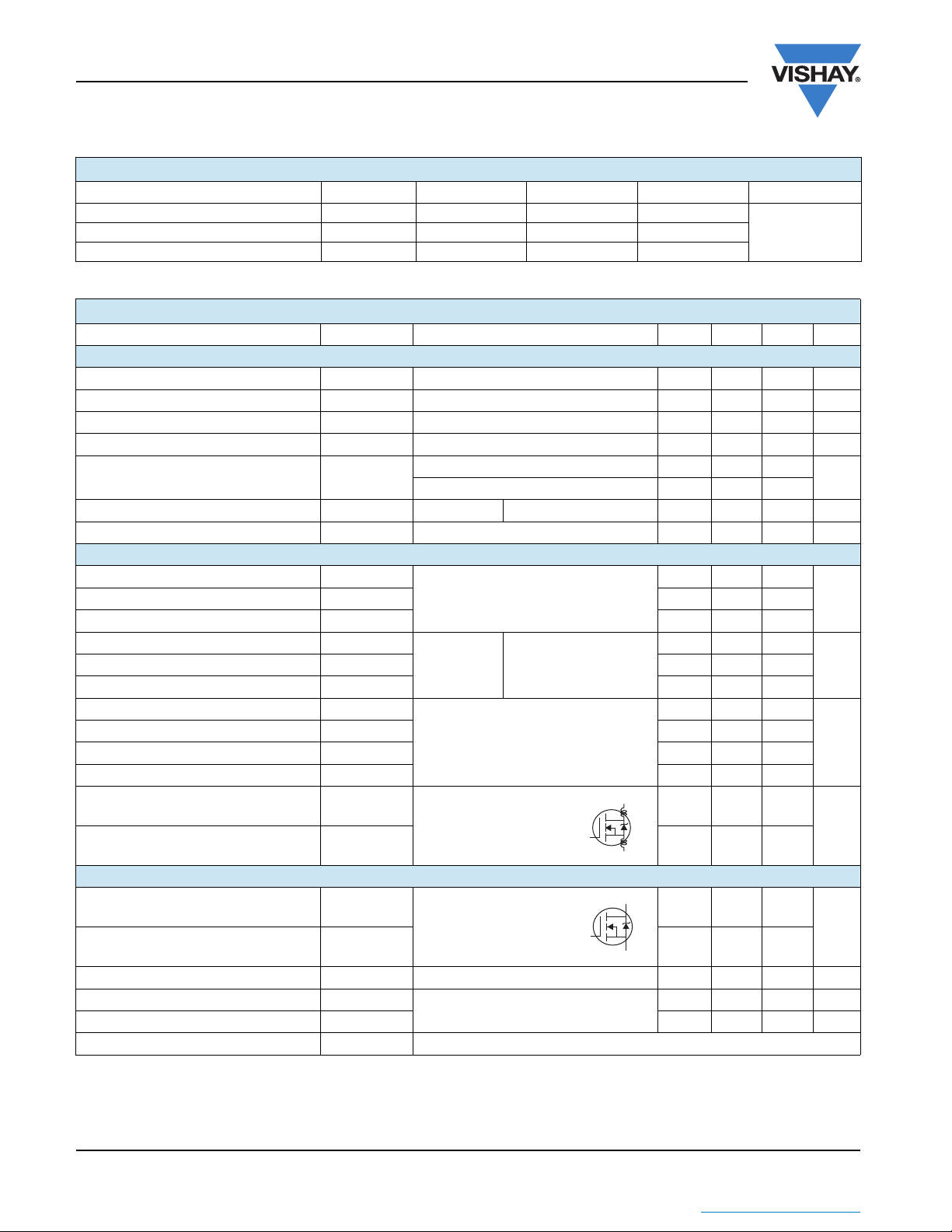
THERMAL RESISTANCE
PARAMETER SYMBOL MIN. TYP. MAX. UNIT
Maximum Junction-to-Ambient R
thJA
--40
°C/WCase-to-Sink, Flat, Greased Surface R
thCS
-0.24-
Maximum Junction-to-Case (Drain) R
thJC
- - 0.65
SPECIFICATIONS (T
J
= 25 °C, unless otherwise noted)
PARAMETER SYMBOL TEST CONDITIONS MIN. TYP. MAX. UNIT
Static
Drain-Source Breakdown Voltage V
DS
V
GS
= 0 V, I
D
= 250 μA 600 - - V
V
DS
Temperature Coefficient ΔV
DS
/T
J
Reference to 25 °C, I
D
= 1 mA - 0.78 - V/°C
Gate-Source Threshold Voltage V
GS(th)
V
DS
= V
GS
, I
D
= 250 μA 2.0 - 4.0 V
Gate-Source Leakage I
GSS
V
GS
= ± 20 V - - ± 100 nA
Zero Gate Voltage Drain Current I
DSS
V
DS
= 600 V, V
GS
= 0 V - - 100
μA
V
DS
= 480 V, V
GS
= 0 V, T
J
= 125 °C - - 500
Drain-Source On-State Resistance R
DS(on)
V
GS
= 10 V I
D
= 6.0 A
b
- - 0.60 Ω
Forward Transconductance g
fs
V
DS
= 100 V, I
D
= 6.0 A
b
5.7 - - S
Dynamic
Input Capacitance C
iss
V
GS
= 0 V,
V
DS
= 25 V,
f = 1.0 MHz, see fig. 5
- 2700 -
pFOutput Capacitance C
oss
- 300 -
Reverse Transfer Capacitance C
rss
-61-
Total Gate Charge Q
g
V
GS
= 10 V
I
D
= 11 A, V
DS
= 360 V
see fig. 6 and 13
b
- - 140
nC Gate-Source Charge Q
gs
--20
Gate-Drain Charge Q
gd
--69
Turn-On Delay Time t
d(on)
V
DD
= 300 V, I
D
= 11 A,
R
g
= 6.2 Ω, R
D
= 30 Ω, see fig. 10
b
-18-
ns
Rise Time t
r
-37-
Turn-Off Delay Time t
d(off)
-88-
Fall Time t
f
-36-
Internal Drain Inductance L
D
Between lead,
6 mm (0.25") from
package and center of
die contact
-5.0-
nH
Internal Source Inductance L
S
-13-
Drain-Source Body Diode Characteristics
Continuous Source-Drain Diode Current I
S
MOSFET symbol
showing the
integral reverse
p - n junction diode
--11
A
Pulsed Diode Forward Current
a
I
SM
--44
Body Diode Voltage V
SD
T
J
= 25 °C, I
S
= 11 A, V
GS
= 0 V
b
--1.4V
Body Diode Reverse Recovery Time t
rr
T
J
= 25 °C, I
F
= 11 A, dI/dt = 100 A/μs
b
- 550 830 ns
Body Diode Reverse Recovery Charge Q
rr
-3.95.9μC
Forward Turn-On Time t
on
Intrinsic turn-on time is negligible (turn-on is dominated by L
S
and L
D
)
D
S
G
S
D
G
器件 Datasheet 文档搜索
AiEMA 数据库涵盖高达 72,405,303 个元件的数据手册,每天更新 5,000 多个 PDF 文件
