Datasheet 搜索 > LED驱动器 > National Semiconductor(美国国家半导体) > LM3224MM-ADJ 数据手册 > LM3224MM-ADJ 产品手册 4/18 页
 器件3D模型
¥ 2.761
LM3224MM-ADJ 产品手册 - National Semiconductor(美国国家半导体)
制造商:
National Semiconductor(美国国家半导体)
分类:
LED驱动器
封装:
MSOP-8
描述:
DC-DC芯片/LM3224MM-ADJ
Pictures:
3D模型
符号图
焊盘图
引脚图
产品图
页面导航:
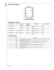
引脚图在P2Hot
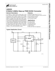
典型应用电路图在P1
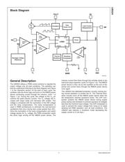
原理图在P3
封装尺寸在P2P18
型号编码规则在P2
封装信息在P2
功能描述在P1P3
技术参数、封装参数在P4
应用领域在P1P10
电气规格在P4P5P6P7P8P10P11
导航目录
LM3224MM-ADJ数据手册
Page:
of 18 Go
若手册格式错乱,请下载阅览PDF原文件
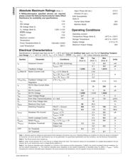
Absolute Maximum Ratings (Note 1)
If Military/Aerospace specified devices are required,
please contact the National Semiconductor Sales Office/
Distributors for availability and specifications.
V
IN
7.5V
SW Voltage 21V
FB Voltage (Note 2) 7V
V
C
Voltage (Note 3) 1.26V
±
0.3V
SHDN Voltage
7.5V
FSLCT 7.5V
Maximum Junction
Temperature
150˚C
Power Dissipation(Note 4) Internally Limited
Lead Temperature 300˚C
Vapor Phase (60 sec.) 215˚C
Infrared (15 sec.) 220˚C
ESD Susceptibility
(Note 5)
Human Body Model 2kV
Machine Model 200V
Operating Conditions
Operating Junction
Temperature Range (Note 6) −40˚C to +125˚C
Storage Temperature −65˚C to +150˚C
Supply Voltage 2.7V to 7V
Maximum Output Voltage 20V
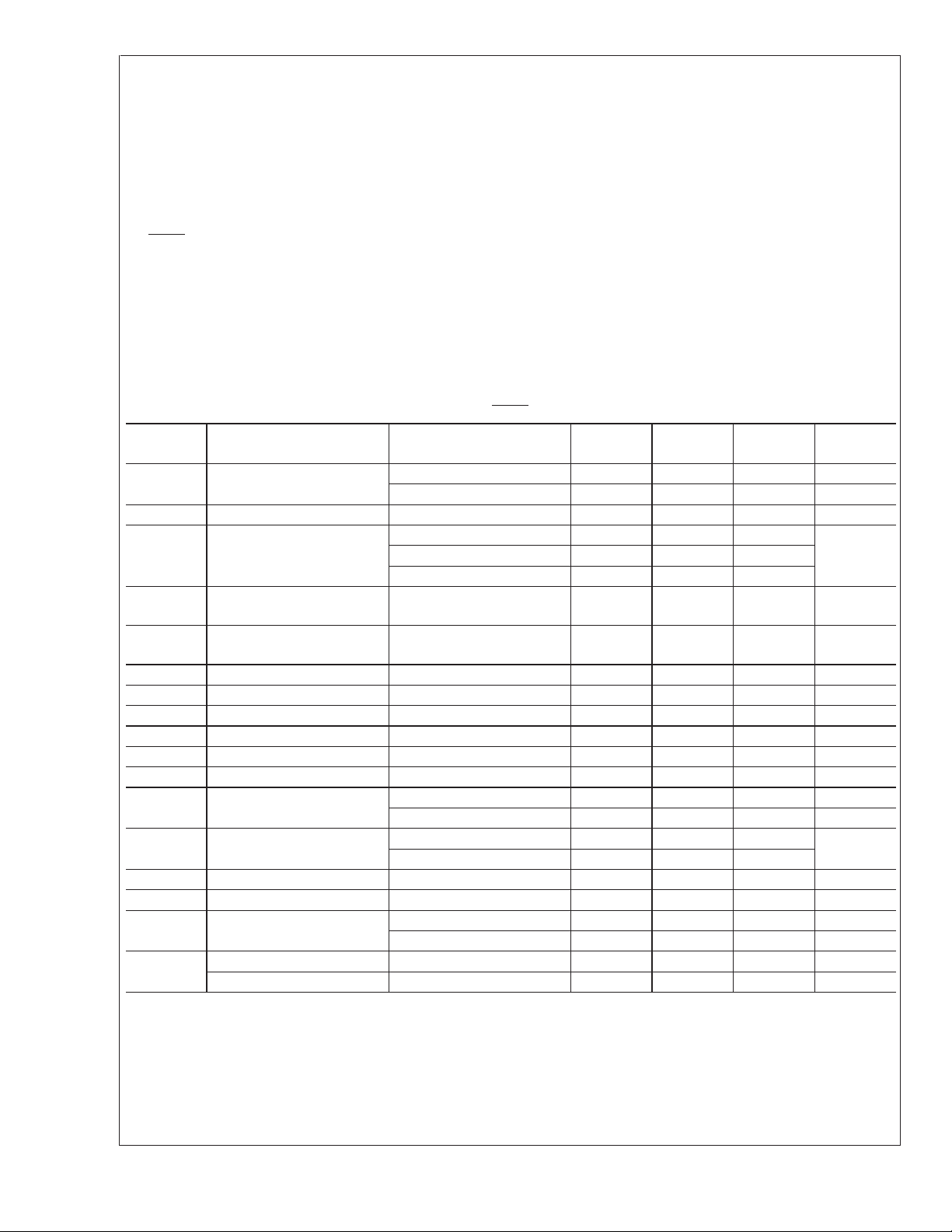
Electrical Characteristics
Specifications in standard type face are for T
J
= 25˚C and those with boldface type apply over the full Operating Tempera-
ture Range (T
J
= −40˚C to +125˚C). V
IN
= 2.7V, FSLCT = SHDN = V
IN
, and I
L
= 0A, unless otherwise specified.
Symbol Parameter Conditions
Min
(Note 6)
Typ
(Note 7)
Max
(Note 6)
Units
I
Q
Quiescent Current FB = 2V (Not Switching) 1.3 2.0 mA
V
SHDN
= 0V 0.1 2.0 µA
V
FB
Feedback Voltage 1.2285 1.26 1.2915 V
I
CL
(Note 8) Switch Current Limit V
IN
= 2.7V (Note 9) 2.45
AV
IN
= 3V, V
OUT
= 8V 2.1
V
IN
= 3V, V
OUT
= 5V 2.2
%V
FB
/∆V
IN
Feedback Voltage Line
Regulation
2.7V ≤ V
IN
≤ 7V
0.085 0.15 %/V
I
B
FB Pin Bias Current (Note
10)
35 250 nA
I
SS
SS Pin Current 7.5 11 13 µA
V
SS
SS Pin Voltage 1.2090 1.2430 1.2622
V
IN
Input Voltage Range 2.7 7 V
g
m
Error Amp Transconductance ∆I = 5µA 40 87 135 µmho
A
V
Error Amp Voltage Gain 78 V/V
D
MAX
Maximum Duty Cycle 85 92.5 %
f
S
Switching Frequency FSLCT = Ground 450 615 750 kHz
FSLCT = V
IN
0.9 1.25 1.5 MHz
I
SHDN
Shutdown Pin Current V
SHDN
= 2.7V 2.4 5.0 µA
V
SHDN
= 0.3V 0.3 1.2
I
L
Switch Leakage Current V
SW
= 20V 0.2 8.0 µA
R
DSON
Switch R
DSON
V
IN
= 2.7V, I
SW
= 1A 0.15 0.4 Ω
Th
SHDN
Shutdown Threshold Output High 1.2 0.8 V
Output Low 0.8 0.3 V
UVP On Threshold 2.3 2.5 V
Off Threshold 2.6 2.7 V
Note 1: Absolute maximum ratings are limits beyond which damage to the device may occur. Operating Ratings are conditions for which the device is intended to
be functional, but device parameter specifications may not be guaranteed. For guaranteed specifications and test conditions, see the Electrical Characteristics.
Note 2: The FB pin should never exceed V
IN
.
Note 3: Under normal operation the V
C
pin may go to voltages above this value. This maximum rating is for the possibility of a voltage being applied to the pin,
however the V
C
pin should never have a voltage directly applied to it.
Note 4: The maximum allowable power dissipation is a function of the maximum junction temperature, T
J
(MAX), the junction-to-ambient thermal resistance, θ
JA
,
and the ambient temperature, T
A
. The maximum allowable power dissipation at any ambient temperature is calculated using: P
D
(MAX) = (T
J(MAX)
−T
A
)/θ
JA
.
Exceeding the maximum allowable power dissipation will cause excessive die temperature, and the regulator will go into thermal shutdown.
LM3224
www.national.com 4
器件 Datasheet 文档搜索
AiEMA 数据库涵盖高达 72,405,303 个元件的数据手册,每天更新 5,000 多个 PDF 文件
