Datasheet 搜索 > 音频放大器 > TI(德州仪器) > LM4940TSX/NOPB 数据手册 > LM4940TSX/NOPB 其他数据使用手册 2/22 页

¥ 20.583
LM4940TSX/NOPB 其他数据使用手册 - TI(德州仪器)
制造商:
TI(德州仪器)
分类:
音频放大器
封装:
TO-263-9
描述:
6W立体声音频功率放大器 6W Stereo Audio Power Amplifier
Pictures:
3D模型
符号图
焊盘图
引脚图
产品图
页面导航:
引脚图在P2Hot
典型应用电路图在P1
原理图在P9
封装尺寸在P2P21
型号编码规则在P2P21
封装信息在P2
功能描述在P1P10
技术参数、封装参数在P4P6
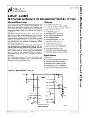
应用领域在P1
电气规格在P3P4P6P7
导航目录
LM4940TSX/NOPB数据手册
Page:
of 22 Go
若手册格式错乱,请下载阅览PDF原文件
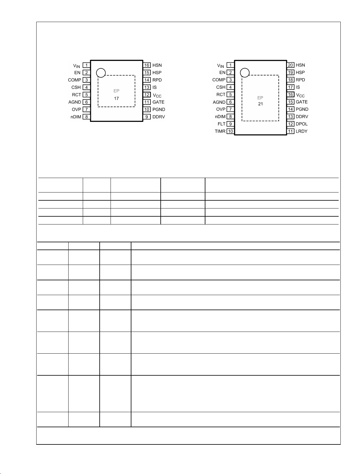
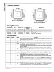
Connection Diagrams
Top View
30067304
16-Lead TSSOP EP
NS Package Number MXA16A
Top View
30067366
20-Lead TSSOP EP
NS Package Number MXA20A
Ordering Information
Order Number Spec. Package Type NSC Package
Drawing
Supplied As
LM3421MH NOPB TSSOP-16 EP MXA16A 92 Units, Rail
LM3421MHX NOPB TSSOP-16 EP MXA16A 2500 Units, Tape and Reel
LM3423MH NOPB TSSOP-20 EP MXA20A 73 Units, Rail
LM3423MHX NOPB TSSOP-20 EP MXA20A 2500 Units, Tape and Reel
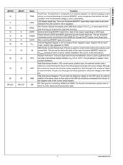
Pin Descriptions
LM3423 LM3421 Name Function
1 1
V
IN
Power supply input (4.5V-75V). Bypass with 100nF capacitor to AGND as close to the device
as possible in the circuit board layout.
2 2 EN
Enable: Pull to ground for zero current shutdown. Tie directly to V
IN
for automatic startup at
4.1V.
3 3 COMP
Compensation: PWM controller error amplifier compensation pin. This pin connects through
a series resistor-capacitor network to AGND.
4 4 CSH
Current Sense High: Output of the high side sense amplifier and input to the main regulation
loop error amplifier.
5 5 RCT
Resistor Capacitor Timing: External RC network sets the predictive “off-time” and thus the
switching frequency. The RC network should be placed as close to the device as possible in
the circuit board layout.
6 6 AGND
Analog Ground: The proper place to connect the compensation and timing capacitor returns.
This pin should be connected via the circuit board to the PGND pin through the EP copper
circuit board pad.
7 7 OVP
Over-Voltage Protection sense input: 1.24V threshold with hysteresis that is user
programmable by the selection of the OVP Over-Voltage Lock-Out (OVLO) resistor divider
network.
8 8 nDIM
Not DIM input: Dual function pin. Primarily used as the Pulse Width Modulation (PWM) input.
When driven with a resistor divider from V
IN
, this pin also functions as a user programmable
V
IN
Under-Voltage Lock-Out (UVLO) with 1.24V threshold and programmable hysteresis by
the UVLO resistor divider network. The PWM and UVLO functions can be performed
simultaneously.
9 - FLT
Fault flag: This is an N-channel MOSFET open drain output. The FLT pin transitions to the
high (open) state once the Fault Timer has timed out and latched the controller off.
www.national.com 2
LM3421, LM3423
器件 Datasheet 文档搜索
AiEMA 数据库涵盖高达 72,405,303 个元件的数据手册,每天更新 5,000 多个 PDF 文件
