Datasheet 搜索 > FET驱动器 > TI(德州仪器) > LM5110-1SDX/NOPB 数据手册 > LM5110-1SDX/NOPB 其他数据使用手册 1/26 页

¥ 19.64
LM5110-1SDX/NOPB 其他数据使用手册 - TI(德州仪器)
制造商:
TI(德州仪器)
分类:
FET驱动器
封装:
WDFN-10
描述:
具有 4V UVLO、专用输入接地和关断输入的 5A/3A 双通道栅极驱动器 10-WSON -40 to 125
Pictures:
3D模型
符号图
焊盘图
引脚图
产品图
页面导航:
导航目录
LM5110-1SDX/NOPB数据手册
Page:
of 26 Go
若手册格式错乱,请下载阅览PDF原文件
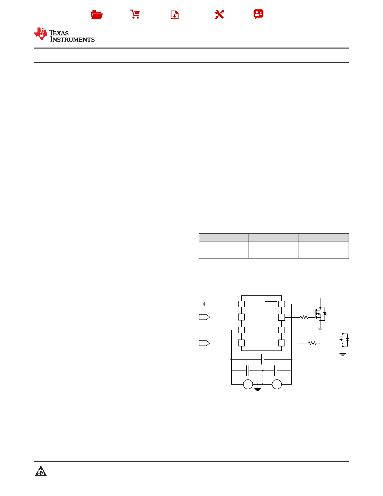
LM5110
1
2
3
4
8
7
6
5
IN_REF
IN_A
IN_B
VEE
SHDN
OUT_A
OUT_B
VCC
1.0F
INA
0.1F
R
G
R
G
INB
0.1F
+
±
+
±
V
POS
V
NEG
Copyright © 2016, Texas Instruments Incorporated
Product
Folder
Sample &
Buy
Technical
Documents
Tools &
Software
Support &
Community
An IMPORTANT NOTICE at the end of this data sheet addresses availability, warranty, changes, use in safety-critical applications,
intellectual property matters and other important disclaimers. PRODUCTION DATA.
LM5110
SNVS255B –MAY 2004–REVISED SEPTEMBER 2016
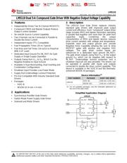
LM5110 Dual 5-A Compound Gate Driver With Negative Output Voltage Capability
1
1 Features
1
• Independently Drives Two N-Channel MOSFETs
• Compound CMOS and Bipolar Outputs Reduce
Output Current Variation
• 5A sink/3A Source Current Capability
• Two Channels can be Connected in Parallel to
Double the Drive Current
• Independent Inputs (TTL Compatible)
• Fast Propagation Times (25-ns Typical)
• Fast Rise and Fall Times (14-ns/12-ns Rise/Fall
With 2-nF Load)
• Dedicated Input Ground Pin (IN_REF) for Split
Supply or Single Supply Operation
• Outputs Swing from V
CC
to V
EE
Which Can Be
Negative Relative to Input Ground
• Available in Dual Noninverting, Dual Inverting and
Combination Configurations
• Shutdown Input Provides Low Power Mode
• Supply Rail Undervoltage Lockout Protection
• Pin-Out Compatible With Industry Standard Gate
Drivers
• Packages:
– SOIC-8
– WSON-10 (4 mm × 4 mm)
2 Applications
• Synchronous Rectifier Gate Drivers
• Switch-Mode Power Supply Gate Driver
• Solenoid and Motor Drivers
3 Description
The LM5110 Dual Gate Driver replaces industry
standard gate drivers with improved peak output
current and efficiency. Each “compound” output driver
stage includes MOS and bipolar transistors operating
in parallel that together sink more than 5A peak from
capacitive loads. Combining the unique
characteristics of MOS and bipolar devices reduces
drive current variation with voltage and temperature.
Separate input and output ground pins provide
Negative Drive Capability allowing the user to drive
MOSFET gates with positive and negative VGS
voltages. The gate driver control inputs are
referenced to a dedicated input ground (IN_REF).
The gate driver outputs swing from V
CC
to the output
ground V
EE
which can be negative with respect to
IN_REF. Undervoltage lockout protection and a
shutdown input pin are also provided. The drivers can
be operated in parallel with inputs and outputs
connected to double the drive current capability. This
device is available in the SOIC-8 and the thermally-
enhanced WSON-10 packages.
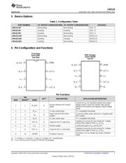
Device Information
(1)
PART NUMBER PACKAGE BODY SIZE (NOM)
LM5110
SOIC (8) 4.90 mm × 3.91 mm
WSON (10) 4.00 mm × 4.00 mm
(1) For all available packages, see the orderable addendum at
the end of the data sheet.
Simplified Application Diagram
器件 Datasheet 文档搜索
AiEMA 数据库涵盖高达 72,405,303 个元件的数据手册,每天更新 5,000 多个 PDF 文件
