Datasheet 搜索 > FET驱动器 > TI(德州仪器) > LM5112MY/NOPB 数据手册 > LM5112MY/NOPB 其他数据使用手册 1/21 页

¥ 8.041
LM5112MY/NOPB 其他数据使用手册 - TI(德州仪器)
制造商:
TI(德州仪器)
分类:
FET驱动器
封装:
PowerPad-MSOP-8
描述:
TEXAS INSTRUMENTS LM5112MY/NOPB 驱动器, MOSFET, 低压侧, 3.5V-14V电源, 7A输出, 25ns延迟, MSOP-8
Pictures:
3D模型
符号图
焊盘图
引脚图
产品图
页面导航:
引脚图在P3Hot
典型应用电路图在P11P12
原理图在P1P8
封装尺寸在P17P19P20
标记信息在P17P18
封装信息在P16P17P18P19P20
技术参数、封装参数在P4
应用领域在P1P21
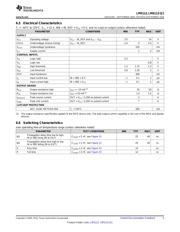
电气规格在P5

导航目录
LM5112MY/NOPB数据手册
Page:
of 21 Go
若手册格式错乱,请下载阅览PDF原文件
Copyright © 2016, Texas Instruments Incorporated
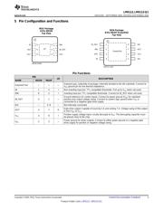
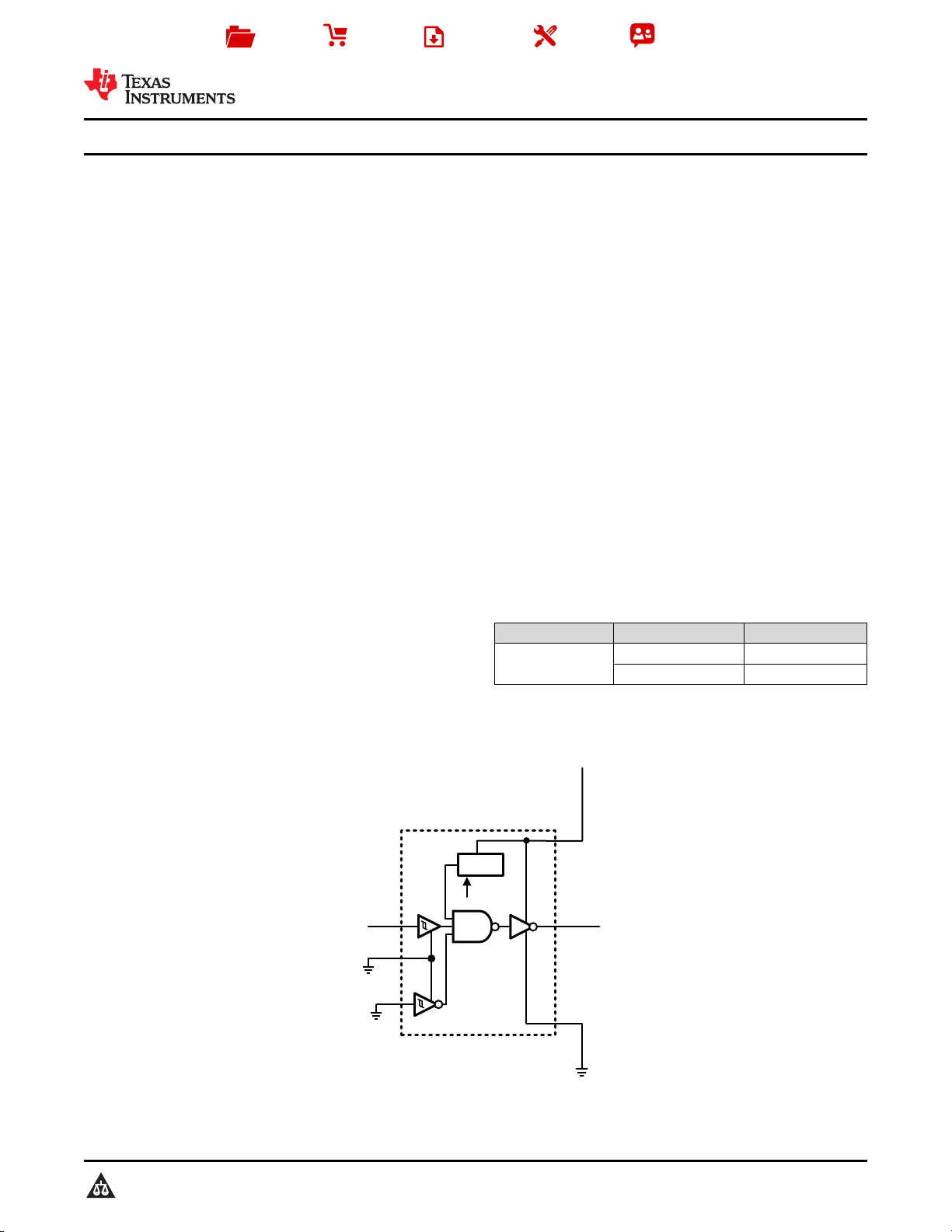
IN
INB
OUT
V
EE
IN_REF
LM5112
V
CC
UVLO
IN_REF
Product
Folder
Sample &
Buy
Technical
Documents
Tools &
Software
Support &
Community
An IMPORTANT NOTICE at the end of this data sheet addresses availability, warranty, changes, use in safety-critical applications,
intellectual property matters and other important disclaimers. PRODUCTION DATA.
LM5112
,
LM5112-Q1
SNVS234C –SEPTEMBER 2004–REVISED SEPTEMBER 2016
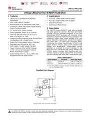
LM5112, LM5112-Q1 Tiny 7-A MOSFET Gate Driver
1
1 Features
1
• LM5112-Q1 is Qualified for Automotive
Applications
• AEC-Q100 Grade 1 Qualified
• Manufactured on an Automotive Grade Flow
• Compound CMOS and Bipolar Outputs Reduce
Output Current Variation
• 7-A Sink and 3-A Source Current
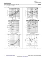
• Fast Propagation Times: 25 ns (Typical)
• Fast Rise and Fall Times: 14 ns or 12 ns
Rise or Fall With 2-nF Load
• Inverting and Non-Inverting Inputs Provide Either
Configuration With a Single Device
• Supply Rail Undervoltage Lockout Protection
• Dedicated Input Ground (IN_REF) for
Split Supply or Single Supply Operation
• Power Enhanced 6-Pin WSON Package
(3 mm × 3 mm) or Thermally Enhanced
MSOP-PowerPAD Package
• Output Swings From V
CC
to V
EE
Which Are
Negative Relative to Input Ground
2 Applications
• DC to DC Switch-Mode Power Supplies
• AC to DC Switch-Mode Power Supplies
• Solar Microinverters
• Solenoid and Motor Drives
3 Description
The LM5112 device MOSFET gate driver provides
high peak gate drive current in the tiny 6-pin WSON
package (SOT-23 equivalent footprint) or an 8-pin
exposed-pad MSOP package with improved power
dissipation required for high frequency operation. The
compound output driver stage includes MOS and
bipolar transistors operating in parallel that together
sink more than 7 A peak from capacitive loads.
Combining the unique characteristics of MOS and
bipolar devices reduces drive current variation with
voltage and temperature. Undervoltage lockout
protection is provided to prevent damage to the
MOSFET due to insufficient gate turnon voltage. The
LM5112 device provides both inverting and non-
inverting inputs to satisfy requirements for inverting
and non-inverting gate drive with a single device type.
Device Information
(1)
PART NUMBER PACKAGE BODY SIZE (NOM)
LM5112,
LM5112-Q1
WSON (6) 3.00 mm × 3.00 mm
MSOP PowerPAD (8) 3.00 mm × 3.00 mm
(1) For all available packages, see the orderable addendum at
the end of the data sheet.
Simplified Block Diagram
器件 Datasheet 文档搜索
AiEMA 数据库涵盖高达 72,405,303 个元件的数据手册,每天更新 5,000 多个 PDF 文件
