Datasheet 搜索 > 放大器、缓冲器 > TI(德州仪器) > LMC6001BIN 数据手册 > LMC6001BIN 其他数据使用手册 4/14 页
 器件3D模型
¥ 59.589
LMC6001BIN 其他数据使用手册 - TI(德州仪器)
制造商:
TI(德州仪器)
分类:
放大器、缓冲器
封装:
DIP-8
Pictures:
3D模型
符号图
焊盘图
引脚图
产品图
页面导航:
典型应用电路图在P1P11P12
封装尺寸在P13P14
型号编码规则在P12
封装信息在P12
功能描述在P1
技术参数、封装参数在P2P4
应用领域在P1P11P12
电气规格在P2P3P4P5P6P7P8
导航目录
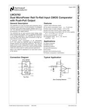
LMC6001BIN数据手册
Page:
of 14 Go
若手册格式错乱,请下载阅览PDF原文件

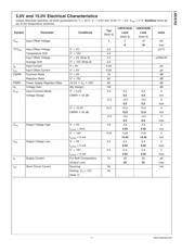
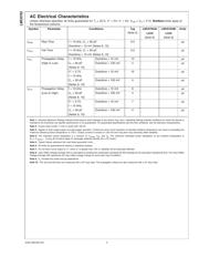
AC Electrical Characteristics
Unless otherwise specified, all limits guaranteed for T
J
= 25˚C, V
+
= 5V, V
−
= 0V, V
CM
=V
O
=V
+
/2. Boldface limits apply at
the temperature extreme.
Symbol Parameter Conditions Typ
(Note 5)
LMC6762AI LMC6762BI Units
Limit Limit
(Note 6) (Note 6)
t
RISE
Rise Time f = 10 kHz, C
L
= 50 pF, 0.3 µs
Overdrive = 10 mV (Notes 9, 10)
t
FALL
Fall Time f = 10 kHz, C
L
= 50 pF, 0.3 µs
Overdrive = 10 mV (Notes 9, 10)
t
PHL
Propagation Delay f = 10 kHz, Overdrive = 10 mV 10 µs
(High to Low) C
L
= 50 pF Overdrive = 100 mV 4 µs
(Notes 9, 10)
V
+
= 2.7V, Overdrive = 10 mV 10 µs
f = 10 kHz,
C
L
= 50 pF Overdrive = 100 mV 4 µs
(Notes 9, 10)
t
PLH
Propagation Delay f = 10 kHz, Overdrive = 10 mV 6 µs
(Low to High) C
L
= 50 pF Overdrive = 100 mV 4 µs
(Notes 9, 10)
V
+
= 2.7V, Overdrive = 10 mV 7 µs
f = 10 kHz,
C
L
= 50 pF Overdrive = 100 mV 4 µs
(Notes 9, 10)
Note 1: Absolute Maximum Ratings indicate limits beyond which damage to the device may occur. Operating Ratings indicate conditions for which the device is
intended to be functional, but specific performance is not guaranteed. For guaranteed specifications and the test conditions, see the electrical characteristics.
Note 2: Human body model, 1.5 kΩ in series with 100 pF.
Note 3: Applies to both single-supply and split-supply operation. Continuous short circuit operation at elevated ambient temperature can result in exceeding the
maximum allowed junction temperature of 150˚C. Output currents in excess of
±
30 mA over long term may adversely affect reliability.
Note 4: The maximum power dissipation is a function of T
J(max)
, θ
JA
, and T
A
. The maximum allowable power dissipation at any ambient temperature is
P
D
=(T
J(max)
–T
A
)/θ
JA
.All numbers apply for packages soldered directly into a PC board.
Note 5: Typical Values represent the most likely parametric norm.
Note 6: All limits are guaranteed by testing or statistical analysis.
Note 7: Do not short circuit output to V
+
, when V
+
is greater than 12V or reliability will be adversely affected.
Note 8: Input Offset Voltage Average Drift is calculated by dividing the accelerated operating life drift average by the equivalent operational time. The Input Offset
Voltage Average Drift represents the input offset voltage change at worst-case input conditions.
Note 9: C
L
includes the probe and jig capacitance.
Note 10: The rise and fall times are measured with a 2V input step. The propagation delays are also measured with a 2V input step.
LMC6762
www.national.com 4
器件 Datasheet 文档搜索
AiEMA 数据库涵盖高达 72,405,303 个元件的数据手册,每天更新 5,000 多个 PDF 文件
