Datasheet 搜索 > 放大器、缓冲器 > TI(德州仪器) > LMC660AIM 数据手册 > LMC660AIM 产品手册 2/18 页

 器件3D模型
¥ 8.883
LMC660AIM 产品手册 - TI(德州仪器)
制造商:
TI(德州仪器)
分类:
放大器、缓冲器
封装:
SOIC-14
描述:
失调电压经改进的四路 15.5V、1.4MHz、CMOS 运算放大器 14-SOIC -40 to 85
Pictures:
3D模型
符号图
焊盘图
引脚图
产品图
页面导航:
封装尺寸在P18
型号编码规则在P1
标记信息在P1
封装信息在P1P16P17
功能描述在P1
技术参数、封装参数在P2P6
应用领域在P1P14
电气规格在P2P3P4P5P6P7P8P9P10P11P12P13
导航目录
LMC660AIM数据手册
Page:
of 18 Go
若手册格式错乱,请下载阅览PDF原文件
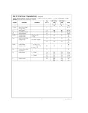
Absolute Maximum Ratings (Note 1)
If Military/Aerospace specified devices are required,
please contact the National Semiconductor Sales Office/
Distributors for availability and specifications.
ESD Tolerance (Note 2) 2000V
Difference Input Voltage
±
Supply Voltage
Voltage at Input/Output Pin (V
+
) + 0.3V, (V
−
) − 0.3V
Supply Voltage (V
+
−V
−
) 16V
Current at Input Pin
±
5mA
Current at Output Pin (Note 3)
±
35 mA
Current at Power Supply Pin 35 mA
Lead Temp. (Soldering, 10 sec.) 260˚C
Storage Temperature Range −65˚C to +150˚C
Junction Temperature (Note 4) 150˚C
Recommended Operating
Conditions
(Note 1)
Supply Voltage 2.7V ≤ V
+
≤ 15.5V
Junction Temperature Range
LMC7101AI, LMC7101BI −40˚C ≤ T
J
≤ +85˚C
Thermal Resistance (θ
JA
)
M05A Package, 5-Pin Surface Mt. 325˚C/W
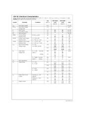
2.7V Electrical Characteristics
Unless otherwise specified, all limits guaranteed for T
J
=
25˚C, V
+
=
2.7V, V
−
=
0V, V
CM
=
V
O
=
V
+
/2 and R
L
>
1MΩ.Bold-
face limits apply at the temperature extremes.
Typ LMC7101AI LMC7101BI
Symbol Parameter Conditions (Note 5) Limit Limit Units
(Note 6) (Note 6)
V
OS
Input Offset Voltage V
+
=
2.7V 0.11 6 9 mV
max
TCV
OS
Input Offset Voltage 1 µV/˚C
Average Drift
I
B
Input Bias Current 1.0 64 64 pA max
I
OS
Input Offset Current 0.5 32 32 pA max
R
IN
Input Resistance
>
1 Tera Ω
CMRR Common-Mode 0V ≤ V
CM
≤ 2.7V 70 55 50 dB
Rejection Ratio V
+
=
2.7V min
V
CM
Input Common-Mode V
+
=
V 0.0 0.0 0.0 V
Voltage Range For CMRR ≥ 50 dB min
3.0 2.7 2.7 V
max
PSRR Power Supply V
+
=
1.35V to 1.65V dB
Rejection Ratio V
−
=
−1.35V to −1.65V 60 50 45 min
V
CM
=
0
C
IN
Common-Mode Input 3 pF
Capacitance
V
O
Output Swing R
L
=
2kΩ 2.45 2.15 2.15 V min
0.25 0.5 0.5 V max
R
L
=
10 kΩ 2.68 2.64 2.64 V min
0.025 0.06 0.06 V max
I
S
Supply Current 0.5 0.81 0.81 mA
0.95 0.95 max
SR Slew Rate (Note 8) 0.7 V/µs
GBW Gain-Bandwidth Product 0.6 MHz
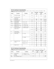
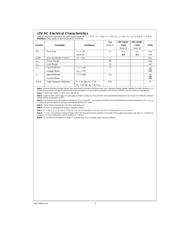
3V DC Electrical Characteristics
Unless otherwise specified, all limits guaranteed for T
J
=
25˚C, V
+
=
3V, V
−
=
0V, V
CM
=
1.5V, V
O
=
V
+
/2 and R
L
=
1MΩ.
Boldface limits apply at the temperature extremes.
Typ LMC7101AI LMC7101BI
Symbol Parameter Conditions (Note 5) Limit Limit Units
(Note 6) (Note 6)
V
OS
Input Offset Voltage 0.11 4 7 mV
www.national.com 2
器件 Datasheet 文档搜索
AiEMA 数据库涵盖高达 72,405,303 个元件的数据手册,每天更新 5,000 多个 PDF 文件
