Datasheet 搜索 > 微控制器 > NXP(恩智浦) > LPC1224FBD64/121,1 数据手册 > LPC1224FBD64/121,1 其他数据使用手册 1/61 页
 器件3D模型
¥ 3.05
LPC1224FBD64/121,1 其他数据使用手册 - NXP(恩智浦)
制造商:
NXP(恩智浦)
分类:
微控制器
封装:
LQFP-64
描述:
NXP LPC1224FBD64/121,1 芯片, MCU, 32位, 48K, 闪存, 4K, 64-LQFP
Pictures:
3D模型
符号图
焊盘图
引脚图
产品图
页面导航:
导航目录
LPC1224FBD64/121,1数据手册
Page:
of 61 Go
若手册格式错乱,请下载阅览PDF原文件

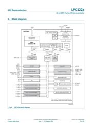
1. General description
The LPC122x extend NXP's 32-bit ARM microcontroller continuum and target a wide
range of industrial applications in the areas of factory and home automation. Benefitting
from the ARM Cortex-M0 Thumb instruction set, the LPC122x have up to 50 % higher
code density compared to common 8/16-bit microcontroller performing typical tasks. The
LPC122x also feature an optimized ROM-based divide library for Cortex-M0, which offers
several times the arithmetic performance of software-based libraries, as well as highly
deterministic cycle time combined with reduced flash code size. The ARM Cortex-M0
efficiency also helps the LPC122x achieve lower average power for similar applications.
The LPC122x operate at CPU frequencies of up to 45 MHz.They offer a wide range of
flash memory options, from 32 kB to 128 kB. The small 512-byte page erase of the flash
memory brings multiple design benefits, such as finer EEPROM emulation, boot-load
support from any serial interface and ease of in-field programming with reduced on-chip
RAM buffer requirements.
The peripheral complement of the LPC122x includes a 10-bit ADC, two comparators with
output feedback loop, two UARTs, one SSP/SPI interface, one I
2
C-bus interface with
Fast-mode Plus features, a Windowed Watchdog Timer, a DMA controller, a CRC engine,
four general purpose timers, a 32-bit RTC, a 1 % internal oscillator for baud rate
generation, and up to 55 General Purpose I/O (GPIO) pins.
2. Features and benefits
Processor core
ARM Cortex-M0 processor, running at frequencies of up to 45 MHz (one wait state
from flash) or 30 MHz (zero wait states from flash). The LPC122x have a high
score of over 45 in CoreMark CPU performance benchmark testing, equivalent to
1.51/MHz.
ARM Cortex-M0 built-in Nested Vectored Interrupt Controller (NVIC).
Serial Wire Debug (SWD).
System tick timer.
Memory
Up to 8 kB SRAM.
Up to 128 kB on-chip flash programming memory.
In-System Programming (ISP) and In-Application Programming (IAP) via on-chip
bootloader software.
Includes ROM-based 32-bit integer division routines.
Clock generation unit
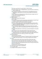
LPC122x
32-bit ARM Cortex-M0 microcontroller; up to 128 kB flash and
8 kB SRAM
Rev. 2 — 26 August 2011 Product data sheet
器件 Datasheet 文档搜索
AiEMA 数据库涵盖高达 72,405,303 个元件的数据手册,每天更新 5,000 多个 PDF 文件
