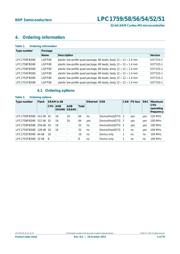
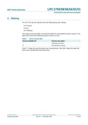
Datasheet 搜索 > 主动器件 > NXP(恩智浦) > LPC1756FBD80 数据手册 > LPC1756FBD80 其他数据使用手册 1/79 页
 器件3D模型
¥ 44.976
LPC1756FBD80 其他数据使用手册 - NXP(恩智浦)
制造商:
NXP(恩智浦)
分类:
主动器件
封装:
LQFP-80
描述:
LPC17xx用户手册 LPC17xx User manual
Pictures:
3D模型
符号图
焊盘图
引脚图
产品图
页面导航:
导航目录
LPC1756FBD80数据手册
Page:
of 79 Go
若手册格式错乱,请下载阅览PDF原文件
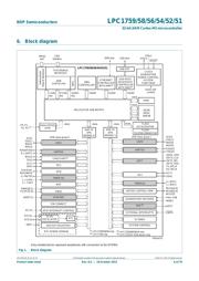
1. General description
The LPC1759/58/56/54/52/51 are ARM Cortex-M3 based microcontrollers for embedded
applications featuring a high level of integration and low power consumption. The ARM
Cortex-M3 is a next generation core that offers system enhancements such as enhanced
debug features and a higher level of support block integration.
The LPC1758/56/57/54/52/51 operate at CPU frequencies of up to 100 MHz. The
LPC1759 operates at CPU frequencies of up to 120 MHz. The ARM Cortex-M3 CPU
incorporates a 3-stage pipeline and uses a Harvard architecture with separate local
instruction and data buses as well as a third bus for peripherals. The ARM Cortex-M3
CPU also includes an internal prefetch unit that supports speculative branching.
The peripheral complement of the LPC1759/58/56/54/52/51 includes up to 512 kB of flash
memory, up to 64 kB of data memory, Ethernet MAC, USB Device/Host/OTG interface,
8-channel general purpose DMA controller, 4 UARTs, 2 CAN channels, 2 SSP controllers,
SPI interface, 2 I
2
C-bus interfaces, 2-input plus 2-output I
2
S-bus interface, 6 channel
12-bit ADC, 10-bit DAC, motor control PWM, Quadrature Encoder interface, 4 general
purpose timers, 6-output general purpose PWM, ultra-low power Real-Time Clock (RTC)
with separate battery supply, and up to 52 general purpose I/O pins.
2. Features and benefits
ARM Cortex-M3 processor, running at frequencies of up to 100 MHz
(LPC1758/56/57/54/52/51) or of up to 120 MHz (LPC1759). A Memory Protection Unit
(MPU) supporting eight regions is included.
ARM Cortex-M3 built-in Nested Vectored Interrupt Controller (NVIC).
Up to 512 kB on-chip flash programming memory. Enhanced flash memory accelerator
enables high-speed 120 MHz operation with zero wait states.
In-System Programming (ISP) and In-Application Programming (IAP) via on-chip
bootloader software.
On-chip SRAM includes:
Up to 32 kB of SRAM on the CPU with local code/data bus for high-performance
CPU access.
Two/one 16 kB SRAM blocks with separate access paths for higher throughput.
These SRAM blocks may be used for Ethernet (LPC1758 only), USB, and DMA
memory, as well as for general purpose CPU instruction and data storage.
Eight channel General Purpose DMA controller (GPDMA) on the AHB multilayer
matrix that can be used with the SSP, I
2
S-bus, UART, the Analog-to-Digital and
Digital-to-Analog converter peripherals, timer match signals, and for
memory-to-memory transfers.
LPC1759/58/56/54/52/51
32-bit ARM Cortex-M3 MCU; up to 512 kB flash and 64 kB
SRAM with Ethernet, USB 2.0 Host/Device/OTG, CAN
Rev. 8.2 — 18 October 2013 Product data sheet
器件 Datasheet 文档搜索
AiEMA 数据库涵盖高达 72,405,303 个元件的数据手册,每天更新 5,000 多个 PDF 文件
