Datasheet 搜索 > 微控制器 > NXP(恩智浦) > LPC1763FBD100K 数据手册 > LPC1763FBD100K 其他数据使用手册 2/90 页
 器件3D模型
¥ 119.108
LPC1763FBD100K 其他数据使用手册 - NXP(恩智浦)
制造商:
NXP(恩智浦)
分类:
微控制器
封装:
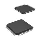
LQFP-100
描述:
ARM MCU微控制单元, LPC Family LPC1700 Series Microcontrollers, ARM 皮质-M3, 32位, 100 MHz, 256 KB, 64 KB
Pictures:
3D模型
符号图
焊盘图
引脚图
产品图
页面导航:
引脚图在P7P8P10P11P12P13P14P15P16P17P18P19Hot
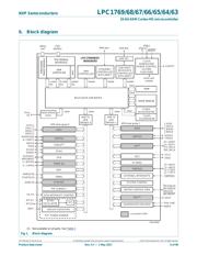
原理图在P6
封装尺寸在P78P79P80
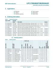
型号编码规则在P4
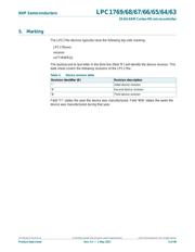
标记信息在P5
焊接温度在P81P82
功能描述在P1P21
技术参数、封装参数在P87
应用领域在P4P87
导航目录
LPC1763FBD100K数据手册
Page:
of 90 Go
若手册格式错乱,请下载阅览PDF原文件

LPC1769_68_67_66_65_64_63 All information provided in this document is subject to legal disclaimers. © NXP Semiconductors N.V. 2017. All rights reserved.
Product data sheet Rev. 9.7 — 1 May 2017 2 of 90
NXP Semiconductors
LPC1769/68/67/66/65/64/63
32-bit ARM Cortex-M3 microcontroller
Two/one 16 kB SRAM blocks with separate access paths for higher throughput.
These SRAM blocks may be used for Ethernet, USB, and DMA memory, as well as
for general purpose CPU instruction and data storage.
Eight channel General Purpose DMA controller (GPDMA) on the AHB multilayer
matrix that can be used with SSP, I
2
S-bus, UART, Analog-to-Digital and
Digital-to-Analog converter peripherals, timer match signals, and for
memory-to-memory transfers.
Multilayer AHB matrix interconnect provides a separate bus for each AHB master.
AHB masters include the CPU, General Purpose DMA controller, Ethernet MAC, and
the USB interface. This interconnect provides communication with no arbitration
delays.
Split APB bus allows high throughput with few stalls between the CPU and DMA.
Serial interfaces:
Ethernet MAC with RMII interface and dedicated DMA controller. (Not available on
all parts, see Table 2
.)
USB 2.0 full-speed device/Host/OTG controller with dedicated DMA controller and
on-chip PHY for device, Host, and OTG functions. (Not available on all parts, see
Table 2
.)
Four UARTs with fractional baud rate generation, internal FIFO, and DMA support.
One UART has modem control I/O and RS-485/EIA-485 support, and one UART
has IrDA support.
CAN 2.0B controller with two channels. (Not available on all parts, see Table 2
.)
SPI controller with synchronous, serial, full duplex communication and
programmable data length.
Two SSP controllers with FIFO and multi-protocol capabilities. The SSP interfaces
can be used with the GPDMA controller.
Three enhanced I
2
C bus interfaces, one with an open-drain output supporting full
I
2
C specification and Fast mode plus with data rates of 1 Mbit/s, two with standard
port pins. Enhancements include multiple address recognition and monitor mode.
I
2
S (Inter-IC Sound) interface for digital audio input or output, with fractional rate
control. The I
2
S-bus interface can be used with the GPDMA. The I
2
S-bus interface
supports 3-wire and 4-wire data transmit and receive as well as master clock
input/output. (Not available on all parts, see Table 2
.)
Other peripherals:
70 (100 pin package) General Purpose I/O (GPIO) pins with configurable
pull-up/down resistors. All GPIOs support a new, configurable open-drain operating
mode. The GPIO block is accessed through the AHB multilayer bus for fast access
and located in memory such that it supports Cortex-M3 bit banding and use by the
General Purpose DMA Controller.
12-bit Analog-to-Digital Converter (ADC) with input multiplexing among eight pins,
conversion rates up to 200 kHz, and multiple result registers. The 12-bit ADC can
be used with the GPDMA controller.
10-bit Digital-to-Analog Converter (DAC) with dedicated conversion timer and DMA
support. (Not available on all parts, see Table 2
)
Four general purpose timers/counters, with a total of eight capture inputs and ten
compare outputs. Each timer block has an external count input. Specific timer
events can be selected to generate DMA requests.
One motor control PWM with support for three-phase motor control.
器件 Datasheet 文档搜索
AiEMA 数据库涵盖高达 72,405,303 个元件的数据手册,每天更新 5,000 多个 PDF 文件
