Datasheet 搜索 > 微控制器 > NXP(恩智浦) > LPC2364FBD100 数据手册 > LPC2364FBD100 其他数据使用手册 1/82 页
 器件3D模型
¥ 49.397
LPC2364FBD100 其他数据使用手册 - NXP(恩智浦)
制造商:
NXP(恩智浦)
分类:
微控制器
封装:
LQFP-100
描述:
ARM7 系列微控制器,NXP一系列 NXP 微控制器,基于 16/32 位 ARM7TDMI-S CPU ,带实时仿真和嵌入式追踪支持,将微控制器与 32 kB、64 kB、128 kB、256 kB 和 512 KB 嵌入式高速闪存相结合。 128 位宽存储器接口和独特的加速器体系结构实现在最大时钟频率时使用 32 位代码。高集成和低功耗 一系列串行通信接口和片上 SRAM 选项 备选 16 位 Thumb 模式将代码缩小 30%,而性能削弱最少。 32 位计时器,PWM 通道和多达 47 条 GPIO 线路 适用于工业控制和医疗系统 ### ARM7/9 微控制器,NXP
Pictures:
3D模型
符号图
焊盘图
引脚图
产品图
页面导航:
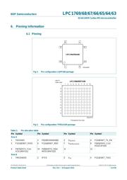
引脚图在P6P8P9P10P11P12P13P14P15P16Hot
原理图在P5
封装尺寸在P73P74
型号编码规则在P4
焊接温度在P75P76
功能描述在P1P18
技术参数、封装参数在P79
应用领域在P4P79
导航目录
LPC2364FBD100数据手册
Page:
of 82 Go
若手册格式错乱,请下载阅览PDF原文件
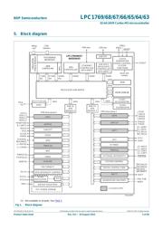
1. General description
The LPC1769/68/67/66/65/64/63 are ARM Cortex-M3 based microcontrollers for
embedded applications featuring a high level of integration and low power consumption.
The ARM Cortex-M3 is a next generation core that offers system enhancements such as
enhanced debug features and a higher level of support block integration.
The LPC1768/67/66/65/64/63 operate at CPU frequencies of up to 100 MHz. The
LPC1769 operates at CPU frequencies of up to 120 MHz. The ARM Cortex-M3 CPU
incorporates a 3-stage pipeline and uses a Harvard architecture with separate local
instruction and data buses as well as a third bus for peripherals. The ARM Cortex-M3
CPU also includes an internal prefetch unit that supports speculative branching.
The peripheral complement of the LPC1769/68/67/66/65/64/63 includes up to 512 kB of
flash memory, up to 64 kB of data memory, Ethernet MAC, USB Device/Host/OTG
interface, 8-channel general purpose DMA controller, 4 UARTs, 2 CAN channels, 2 SSP
controllers, SPI interface, 3 I
2
C-bus interfaces, 2-input plus 2-output I
2
S-bus interface,
8-channel 12-bit ADC, 10-bit DAC, motor control PWM, Quadrature Encoder interface,
four general purpose timers, 6-output general purpose PWM, ultra-low power Real-Time
Clock (RTC) with separate battery supply, and up to 70 general purpose I/O pins.
The LPC1769/68/67/66/65/64/63 are pin-compatible to the 100-pin LPC236x
ARM7-based microcontroller series.
2. Features and benefits
ARM Cortex-M3 processor, running at frequencies of up to 100 MHz
(LPC1768/67/66/65/64/63) or of up to 120 MHz (LPC1769). A Memory Protection Unit
(MPU) supporting eight regions is included.
ARM Cortex-M3 built-in Nested Vectored Interrupt Controller (NVIC).
Up to 512 kB on-chip flash programming memory. Enhanced flash memory accelerator
enables high-speed 120 MHz operation with zero wait states.
In-System Programming (ISP) and In-Application Programming (IAP) via on-chip
bootloader software.
On-chip SRAM includes:
32/16 kB of SRAM on the CPU with local code/data bus for high-performance CPU
access.
LPC1769/68/67/66/65/64/63
32-bit ARM Cortex-M3 microcontroller; up to 512 kB flash and
64 kB SRAM with Ethernet, USB 2.0 Host/Device/OTG, CAN
Rev. 9 — 10 August 2012 Product data sheet
器件 Datasheet 文档搜索
AiEMA 数据库涵盖高达 72,405,303 个元件的数据手册,每天更新 5,000 多个 PDF 文件
