Datasheet 搜索 > 接口芯片 > TI(德州仪器) > MAX3227ECDB 数据手册 > MAX3227ECDB 其他数据使用手册 2/22 页

 器件3D模型
¥ 18.925
MAX3227ECDB 其他数据使用手册 - TI(德州仪器)
制造商:
TI(德州仪器)
分类:
接口芯片
封装:
SSOP-16
描述:
RS-232 Line Transceivers, Single, Texas Instruments### RS-232 线路驱动器和接收器
Pictures:
3D模型
符号图
焊盘图
引脚图
产品图
页面导航:
导航目录
MAX3227ECDB数据手册
Page:
of 22 Go
若手册格式错乱,请下载阅览PDF原文件
MAX3224–MAX3227/MAX3244/MAX3245
†
1µA Supply Current, 1Mbps, 3.0V to 5.5V,
RS-232 Transceivers with AutoShutdown Plus
2 _______________________________________________________________________________________
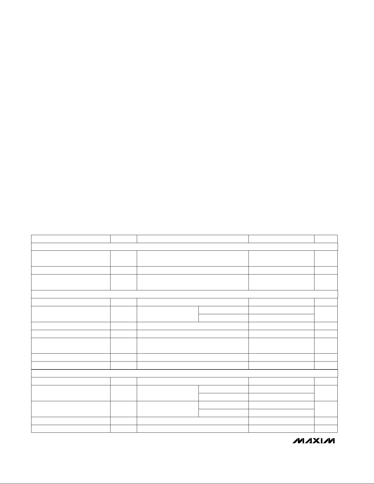
ABSOLUTE MAXIMUM RATINGS
ELECTRICAL CHARACTERISTICS
(V
CC
= +3V to +5.5V, C1–C4 = 0.1µF, tested at 3.3V ±10%; C
L
= 0.047µF, C2–C4 = 0.33µF, tested at 5.0V ±10%; T
A
= T
MIN
to T
MAX
,
unless otherwise noted. Typical values are at T
A
= +25°C.)
Stresses beyond those listed under “Absolute Maximum Ratings” may cause permanent damage to the device. These are stress ratings only, and functional
operation of the device at these or any other conditions beyond those indicated in the operational sections of the specifications is not implied. Exposure to
absolute maximum rating conditions for extended periods may affect device reliability.
V
CC
to GND..............................................................-0.3V to +6V
V+ to GND (Note 1) ..................................................-0.3V to +7V
V- to GND (Note 1) ...................................................+0.3V to -7V
V+ +
V-(Note 1) ................................................................+13V
Input Voltages
T_IN, FORCEON, FORCEOFF to GND ................ -0.3V to +6V
R_IN to GND ....................................................................±25V
Output Voltages
T_OUT to GND.............................................................±13.2V
R_OUT, INVALID, READY to GND .........-0.3V to (V
CC
+ 0.3V)
Short-Circuit Duration
T_OUT to GND .......................................................Continuous
Continuous Power Dissipation (T
A
= +70°C)
16-Pin SSOP (derate 7.14mW/°C above +70°C) .........571mW
20-Pin Plastic DIP (derate 11.11mW/°C above +70°C) ...889mW
20-Pin TQFN (derate 21.3mW/°C above +70°C)........1702.1mW
20-Pin SSOP (derate 8.00mW/°C above +70°C) .........640mW
20-Pin TSSOP (derate 7.00mW/°C above +70°C) .......559mW
28-Pin Wide SO (derate 12.5mW/°C above +70°C)........... 1W
28-Pin SSOP (derate 9.52mW/°C above +70°C) .........762mW
Operating Temperature Ranges
MAX32_ _C_ _....................................................0°C to +70°C
MAX32_ _E_ _..................................................-40°C to +85°C
Storage Temperature Range .............................-65°C to +160°C
Lead Temperature (soldering, 10s) .................................+300°C
Note 1: V+ and V- can have maximum magnitudes of 7V, but their absolute difference cannot exceed 13V.
V
CC
= 5.0V
FORCEON = GND, FORCEOFF = V
CC
,
all R_IN idle, all T_IN idle
T
A
= +25°C
V
CC
= 3.3V
T_IN, FORCEON,
FORCEOFF
CONDITIONS
kΩ357Input Resistance
V0.5Input Hysteresis
1.8 2.4
V
1.5 2.4
Input Threshold High
0.8 1.5
V
0.6 1.2
Input Threshold Low
V-25 +25Input Voltage Range
V
V
CC
- 0.6 V
CC
- 0.1
Output Voltage High
V0.4Output Voltage Low
µA110Supply Current, Shutdown
µA110
Supply Current,
AutoShutdown Plus
µA±0.05 ±10Output Leakage Current
µA±0.01 ±1
Transmitter Input Hysteresis V0.5
V
2.4
Input Logic Threshold High
mA0.3 1
Supply Current,
AutoShutdown Plus Disabled
V0.8Input Logic Threshold Low
2
UNITSMIN TYP MAXSYMBOLPARAMETER
FORCEOFF = GND
T
A
= +25°C
V
CC
= 5.0V
V
CC
= 3.3V
T
A
= +25°C
R_OUT (MAX3244/MAX3245), receivers
disabled
T_IN, FORCEON, FORCEOFF
V
CC
= 5.0V
FORCEON = FORCEOFF = V
CC
, no load
T_IN, FORCEON, FORCEOFF
I
OUT
= -1.0mA
V
CC
= 3.3V
I
OUT
= 1.6mA
DC CHARACTERISTICS (V
CC
= 3.3V or 5.0V, T
A
= +25°C)
LOGIC INPUTS AND RECEIVER OUTPUTS
RECEIVER INPUTS
Input Leakage Current
器件 Datasheet 文档搜索
AiEMA 数据库涵盖高达 72,405,303 个元件的数据手册,每天更新 5,000 多个 PDF 文件
