Datasheet 搜索 > 接口芯片 > Maxim Integrated(美信) > MAX3232EETE+T 数据手册 > MAX3232EETE+T 其他数据使用手册 2/22 页
 器件3D模型
¥ 22.961
MAX3232EETE+T 其他数据使用手册 - Maxim Integrated(美信)
制造商:
Maxim Integrated(美信)
分类:
接口芯片
封装:
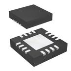
TQFN-16
Pictures:
3D模型
符号图
焊盘图
引脚图
产品图
页面导航:
引脚图在P1P7P8P16P17Hot
典型应用电路图在P1P18P19P20
封装尺寸在P21
型号编码规则在P1P21
封装信息在P15
功能描述在P1
技术参数、封装参数在P21
应用领域在P1P13P15
电气规格在P3
导航目录
MAX3232EETE+T数据手册
Page:
of 22 Go
若手册格式错乱,请下载阅览PDF原文件
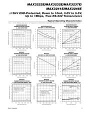
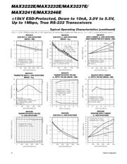
±15kV ESD-Protected, Down to 10nA, 3.0V to 5.5V,
Up to 1Mbps, True RS-232 Transceivers
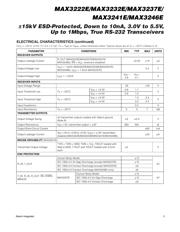
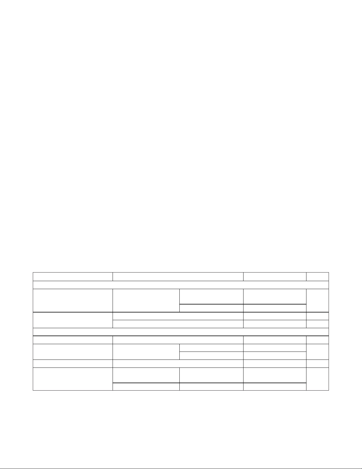
ABSOLUTE MAXIMUM RATINGS
ELECTRICAL CHARACTERISTICS
(V
CC
= +3V to +5.5V, C1–C4 = 0.1µF, T
A
= T
MIN
to T
MAX
, unless otherwise noted. Typical values are at T
A
= +25°C.) (Notes 3, 4)
Stresses beyond those listed under “Absolute Maximum Ratings” may cause permanent damage to the device. These are stress ratings only, and functional
operation of the device at these or any other conditions beyond those indicated in the operational sections of the specifications is not implied. Exposure to
absolute maximum rating conditions for extended periods may affect device reliability.
V
CC
to GND..............................................................-0.3V to +6V
V+ to GND (Note 1) ..................................................-0.3V to +7V
V- to GND (Note 1) ...................................................+0.3V to -7V
V+ + |V-| (Note 1).................................................................+13V
Input Voltages
T_IN, EN, SHDN, MBAUD to GND ........................-0.3V to +6V
R_IN to GND .....................................................................±25V
Output Voltages
T_OUT to GND...............................................................±13.2V
R_OUT, R_OUTB (MAX3237E/MAX3241E)...-0.3V to (V
CC
+ 0.3V)
Short-Circuit Duration, T_OUT to GND.......................Continuous
Continuous Power Dissipation (T
A
= +70°C)
16-Pin SSOP (derate 7.14mW/°C above +70°C) ..........571mW
16-Pin TSSOP (derate 9.4mW/°C above +70°C) .......754.7mW
16-Pin TQFN (derate 20.8mW/°C above +70°C) .....1666.7mW
16-Pin Wide SO (derate 9.52mW/°C above +70°C) .....762mW
18-Pin Wide SO (derate 9.52mW/°C above +70°C) .....762mW
18-Pin PDIP (derate 11.11mW/°C above +70°C)..........889mW
20-Pin TQFN (derate 21.3mW/°C above +70°C) ........1702mW
20-Pin TSSOP (derate 10.9mW/°C above +70°C) ........879mW
20-Pin SSOP (derate 8.00mW/°C above +70°C) ..........640mW
28-Pin SSOP (derate 9.52mW/°C above +70°C) ..........762mW
28-Pin Wide SO (derate 12.50mW/°C above +70°C) .............1W
28-Pin TSSOP (derate 12.8mW/°C above +70°C) ......1026mW
32-Pin TQFN (derate 33.3mW/°C above +70°C)...........2666mW
6 x 6 UCSP (derate 12.6mW/°C above +70°C) .............1010mW
Operating Temperature Ranges
MAX32_ _EC_ _ ...................................................0°C to +70°C
MAX32_ _EE_ _.................................................-40°C to +85°C
Storage Temperature Range .............................-65°C to +150°C
Lead Temperature (soldering, 10s) .................................+300°C
Soldering Temperature (reflow) .......................................+260°C
Bump Reflow Temperature (Note 2)
Infrared, 15s..................................................................+200°C
Vapor Phase, 20s..........................................................+215°C
Note 1: V+ and V- can have maximum magnitudes of 7V, but their absolute difference cannot exceed 13V.
Note 2: This device is constructed using a unique set of packaging techniques that impose a limit on the thermal profile the device
can be exposed to during board-level solder attach and rework. This limit permits only the use of the solder profiles recom-
mended in the industry-standard specification, JEDEC 020A, paragraph 7.6, Table 3 for IR/VPR and convection reflow.
Preheating is required. Hand or wave soldering is not allowed.
PARAMETER CONDITIONS MIN TYP MAX UNITS
DC CHARACTERISTICS (V
CC
= +3.3V or +5V, T
A
= +25°C)
MAX3222E, MAX3232E,
MAX3241E, MAX3246E
0.3 1
Supply Current SHDN = V
CC
, no load
MAX3237E 0.5 2.0
mA
SHDN = GND 1 10 μA
Shutdown Supply Current
SHDN = R_IN = GND, T_IN = GND or V
CC
(MAX3237E) 10 300 nA
LOGIC IN PUTS
Input Logic Low T_IN, EN, SHDN, MBAUD 0.8 V
V
CC
= +3.3V 2.0
Input Logic High T_IN, EN, SHDN, MBAUD
V
CC
= +5.0V 2.4
V
Transmitter Input Hysteresis 0.5 V
T_IN, EN, SHDN
MAX3222E, MAX3232E,
MAX3241E, MAX3246E
±0.01 ±1
Input Leakage Current
T_IN, SHDN, MBAUD MAX3237E (Note 5) 9 18
μA
2
Maxim Integrated
MAX3222E/MAX3232E/MAX3237E/
MAX3241E/MAX3246E
器件 Datasheet 文档搜索
AiEMA 数据库涵盖高达 72,405,303 个元件的数据手册,每天更新 5,000 多个 PDF 文件
