Datasheet 搜索 > 接口芯片 > Maxim Integrated(美信) > MAX4582CSE 数据手册 > MAX4582CSE 其他数据使用手册 1/18 页

 器件3D模型
¥ 7.191
MAX4582CSE 其他数据使用手册 - Maxim Integrated(美信)
制造商:
Maxim Integrated(美信)
分类:
接口芯片
封装:
SOIC-16
描述:
低电压, CMOS模拟多路复用器/开关 Low-Voltage, CMOS Analog Multiplexers/Switches
Pictures:
3D模型
符号图
焊盘图
引脚图
产品图
页面导航:
导航目录
MAX4582CSE数据手册
Page:
of 18 Go
若手册格式错乱,请下载阅览PDF原文件

For pricing delivery, and ordering information please contact Maxim Direct! at 1-888-629-4642,
or visit Maxim’s website at www.maxim-ic.com.
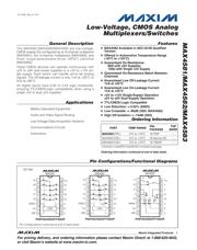
________________General Description
The MAX4581/MAX4582/MAX4583 are low-voltage,
CMOS analog ICs configured as an 8-channel multiplexer
(MAX4581), two 4-channel multiplexers (MAX4582), and
three single-pole/double-throw (SPDT) switches
(MAX4583).
These CMOS devices can operate continuously with
±2V to ±6V dual power supplies or a +2V to +12V sin-
gle supply. Each switch can handle rail-to-rail analog
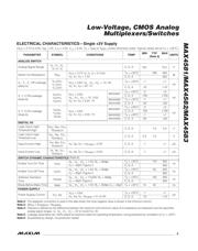
signals. The off-leakage current is only 1nA at +25°C or
5nA at +85°C.
All digital inputs have 0.8V to 2.4V logic thresholds,
ensuring TTL/CMOS-logic compatibility when using a
single +5V or dual ±5V supplies.
________________________Applications
Battery-Operated Equipment
Audio and Video Signal Routing
Low-Voltage Data-Acquisition Systems
Communications Circuits
Automotive
____________________________Features
o MAX4582 Available in AEC-Q100 Qualified
Version
o Offered in Automotive Temperature Range
(-40°C to +125°C)
o Guaranteed On-Resistance
80Ω with ±5V Supplies
150
ΩΩ
with Single +5V Supply
o Guaranteed On-Resistance Match Between
Channels
o Guaranteed Low Off-Leakage Current
1nA at +25°C
o Guaranteed Low On-Leakage Current
1nA at +25°C
o +2V to +12V Single-Supply Operation
±2V to ±6V Dual-Supply Operation
o TTL/CMOS-Logic Compatible
o Low Distortion: < 0.02% (600Ω)
o Low Crosstalk: < -96dB (50Ω, MAX4582)
o High Off-Isolation: < -74dB (50Ω)
MAX4581/MAX4582/MAX4583
Low-Voltage, CMOS Analog
Multiplexers/Switches
________________________________________________________________
Maxim Integrated Products
1
16
15
14
13
12
11
10
9
1
2
3
4
5
6
7
8
V
CC
X2
X1
X0
X3
A
B
C
X4
X6
X
X7
X5
ENABLE
V
EE
GND
TOP VIEW
MAX4581
PDIP/SO/QSOP/TSSOP
LOGIC
16
15
14
13
12
11
10
9
1
2
3
4
5
6
7
8
V
CC
Y
X
X1
X0
A
B
C
Y1
Y0
Z1
Z
Z0
ENABLE
V
EE
GND
MAX4583
PDIP/SO/QSOP/TSSOP
16
15
14
13
12
11
10
9
1
2
3
4
5
6
7
8
V
CC
X2
X1
X
X0
X3
A
B
Y0
Y2
Y
Y3
Y1
ENABLE
V
EE
GND
MAX4582
PDIP/SO/QSOP/TSSOP
LOGIC
++
+
____________________________________Pin Configurations/Functional Diagrams
19-1328; Rev 6; 3/12
Ordering Information continued at end of data sheet.
PART TEMP RANGE
PIN-
PACKAGE
TOP
MARK
MAX4581CPE+ 0°C to +70°C 16 PDIP —
MAX4581CSE+ 0°C to +70°C 16 Narrow SO —
MAX4581CUE+ 0°C to +70°C 16 TSSOP —
Ordering Information
Pin Configurations continued at end of data sheet.
+
Denotes a lead(Pb)-free/RoHS-compliant package.
器件 Datasheet 文档搜索
AiEMA 数据库涵盖高达 72,405,303 个元件的数据手册,每天更新 5,000 多个 PDF 文件
