Datasheet 搜索 > 逻辑芯片 > ON Semiconductor(安森美) > MC14007UBCP 数据手册 > MC14007UBCP 产品封装文件 1/9 页
 器件3D模型
¥ 7.18
MC14007UBCP 产品封装文件 - ON Semiconductor(安森美)
制造商:
ON Semiconductor(安森美)
分类:
逻辑芯片
封装:
DIP-14
描述:
双互补对加变频器 Dual Complementary Pair Plus Inverter
Pictures:
3D模型
符号图
焊盘图
引脚图
产品图
页面导航:
引脚图在P1Hot
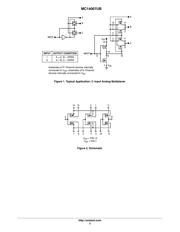
典型应用电路图在P2
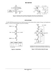
原理图在P2
封装尺寸在P7P8
焊盘布局在P8
型号编码规则在P1P6P8
标记信息在P1P8
封装信息在P6
功能描述在P1
技术参数、封装参数在P4P6
应用领域在P1P5P6
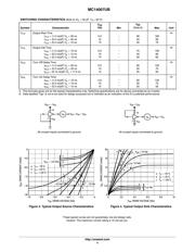
电气规格在P3
导航目录
MC14007UBCP数据手册
Page:
of 9 Go
若手册格式错乱,请下载阅览PDF原文件
© Semiconductor Components Industries, LLC, 2013
April, 2013 − Rev. 10
1 Publication Order Number:
MC14007UB/D
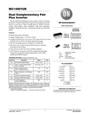
MC14007UB
Dual Complementary Pair
Plus Inverter
The MC14007UB multipurpose device consists of three N−Channel
and three P−Channel enhancement mode devices packaged to provide
access to each device. These versatile parts are useful in inverter
circuits, pulse−shapers, linear amplifiers, high input impedance
amplifiers, threshold detectors, transmission gating, and functional
gating.
Features
• Diode Protection on All Inputs
• Supply Voltage Range = 3.0 Vdc to 18 Vdc
• Capable of Driving Two Low−power TTL Loads or One Low−power
Schottky TTL Load Over the Rated Temperature Range
• Pin−for−Pin Replacement for CD4007A or CD4007UB
• This device has 2 outputs without ESD Protection. Antistatic
precautions must be taken.
• These Devices are Pb−Free and are RoHS Compliant
• NLV Prefix for Automotive and Other Applications Requiring
Unique Site and Control Change Requirements; AEC−Q100
Qualified and PPAP Capable
MAXIMUM RATINGS (Voltages Referenced to V
SS
)
Symbol
Parameter Value Unit
V
DD
DC Supply Voltage Range −0.5 to +18.0 V
V
in
, V
out
Input or Output Voltage Range
(DC or Transient)
−0.5 to V
DD
+0.5 V
I
in
, I
out
Input or Output Current
(DC or Transient) per Pin
± 10 mA
P
D
Power Dissipation, per Package
(Note 1)
500 mW
T
A
Ambient Temperature Range −55 to +125 °C
T
stg
Storage Temperature Range −65 to +150 °C
T
L
Lead Temperature
(8 second Soldering)
260 °C
Stresses exceeding Maximum Ratings may damage the device. Maximum
Ratings are stress ratings only. Functional operation above the Recommended
Operating Conditions is not implied. Extended exposure to stresses above the
Recommended Operating Conditions may affect device reliability.
1. Temperature Derating:
Plastic “P and D/DW” Packages: – 7.0 mW/°C from 65°C 5o 125°C.
See detailed ordering and shipping information in the package
dimensions section on page 6 of this data sheet.
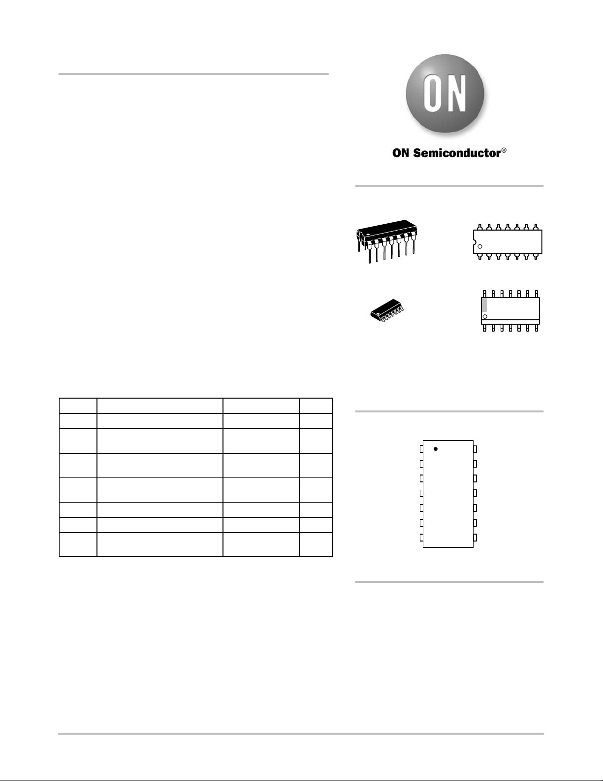
ORDERING INFORMATION
11
12
13
14
8
9
105
4
3
2
1
7
6
GATE
C
S−P
C
OUT
C
D−P
A
V
DD
D−N
A
S−N
C
S−N
B
GATE
B
S−P
B
D−P
B
V
SS
GATE
A
D−N
B
PIN ASSIGNMENT
D = DRAIN
S = SOURCE
MARKING
DIAGRAMS
1
14
PDIP−14
P SUFFIX
CASE 646
MC14007UBCP
AWLYYWWG
SOIC−14
D SUFFIX
CASE 751A
1
14
14007UG
AWLYWW
A = Assembly Location
WL, L = Wafer Lot
YY, Y = Year
WW, W = Work Week
G = Pb−Free Indicator
http://onsemi.com
器件 Datasheet 文档搜索
AiEMA 数据库涵盖高达 72,405,303 个元件的数据手册,每天更新 5,000 多个 PDF 文件
