Datasheet 搜索 > 逻辑芯片 > ON Semiconductor(安森美) > MC14012BDR2 数据手册 > MC14012BDR2 其他数据使用手册 1/9 页
 器件3D模型
¥ 0.223
MC14012BDR2 其他数据使用手册 - ON Semiconductor(安森美)
制造商:
ON Semiconductor(安森美)
分类:
逻辑芯片
封装:
SOIC-14
描述:
B-后缀系列CMOS门 B−Suffix Series CMOS Gates
Pictures:
3D模型
符号图
焊盘图
引脚图
产品图
页面导航:
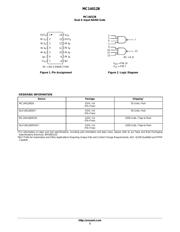
引脚图在P2Hot
典型应用电路图在P2
原理图在P4
封装尺寸在P7
焊盘布局在P7
型号编码规则在P1P2P9
标记信息在P1P7P9
封装信息在P2
技术参数、封装参数在P2
应用领域在P1P2
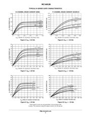
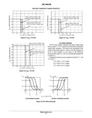
电气规格在P3P6
型号编号列表在P1
导航目录
MC14012BDR2数据手册
Page:
of 9 Go
若手册格式错乱,请下载阅览PDF原文件
© Semiconductor Components Industries, LLC, 2014
July, 2014 − Rev. 11
1 Publication Order Number:
MC14012B/D
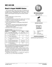
MC14012B
Dual 4-Input NAND Gates
The MC14012B dual 4−input NAND gates are constructed with
P−Channel and N−Channel enhancement mode devices in a single
monolithic structure (Complementary MOS). Their primary use is
where low power dissipation and/or high noise immunity is desired.
Features
• Supply Voltage Range = 3.0 Vdc to 18 Vdc
• All Outputs Buffered
• Capable of Driving Two Low−Power TTL Loads or One Low−Power
Schottky TTL Load Over the Rated Temperature Range
• Double Diode Protection on All Inputs
• Pin−for−Pin Replacements for Corresponding CD4000 Series B
Suffix Devices
• NLV Prefix for Automotive and Other Applications Requiring
Unique Site and Control Change Requirements; AEC−Q100
Qualified and PPAP Capable
• This Device is Pb−Free and is RoHS Compliant
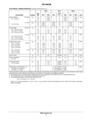
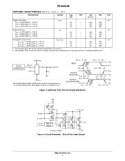
MAXIMUM RATINGS (Voltages Referenced to V
SS
)
Symbol
Parameter Value Unit
V
DD
DC Supply Voltage Range −0.5 to +18.0 V
V
in
, V
out
Input or Output Voltage Range
(DC or Transient)
−0.5 to V
DD
+ 0.5 V
I
in
, I
out
Input or Output Current
(DC or Transient) per Pin
± 10 mA
P
D
Power Dissipation, per Package
(Note 1)
500 mW
T
A
Ambient Temperature Range −55 to +125 °C
T
stg
Storage Temperature Range −65 to +150 °C
T
L
Lead Temperature
(8−Second Soldering)
260 °C
Stresses exceeding those listed in the Maximum Ratings table may damage the
device. If any of these limits are exceeded, device functionality should not be
assumed, damage may occur and reliability may be affected.
1. Temperature Derating: “D/DW” Package: –7.0 mW/_C From 65_C To 125_C
This device contains protection circuitry to guard against damage due to high
static voltages or electric fields. However, precautions must be taken to avoid
applications of any voltage higher than maximum rated voltages to this
high−impedance circuit. For proper operation, V
in
and V
out
should be constrained
to the range V
SS
≤ (V
in
or V
out
) ≤ V
DD
.
Unused inputs must always be tied to an appropriate logic voltage level
(e.g., either V
SS
or V
DD
). Unused outputs must be left open.
MARKING DIAGRAM
SOIC−14
D SUFFIX
CASE 751A
1
14
14012BG
AWLYWW
A = Assembly Location
WL, L = Wafer Lot
YY, Y = Year
WW, W = Work Week
G = Pb−Free Package
See detailed ordering and shipping information in the package
dimensions section on page 2 of this data sheet.
ORDERING INFORMATION
http://onsemi.com
器件 Datasheet 文档搜索
AiEMA 数据库涵盖高达 72,405,303 个元件的数据手册,每天更新 5,000 多个 PDF 文件
