Datasheet 搜索 > 逻辑芯片 > ON Semiconductor(安森美) > MC14025BCP 数据手册 > MC14025BCP 其他数据使用手册 1/6 页
 器件3D模型
¥ 0
MC14025BCP 其他数据使用手册 - ON Semiconductor(安森美)
制造商:
ON Semiconductor(安森美)
分类:
逻辑芯片
封装:
DIP-14
描述:
B-后缀系列CMOS门 B-SUFFIX SERIES CMOS GATES
Pictures:
3D模型
符号图
焊盘图
引脚图
产品图
页面导航:
导航目录
MC14025BCP数据手册
Page:
of 6 Go
若手册格式错乱,请下载阅览PDF原文件
Semiconductor Components Industries, LLC, 2005
February, 2005 − Rev. 5
1 Publication Order Number:
MC14070B/D
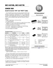
MC14070B, MC14077B
CMOS SSI
Quad Exclusive “OR” and “NOR” Gates
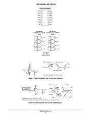
The MC14070B quad exclusive OR gate and the MC14077B quad
exclusive NOR gate are constructed with MOS P−channel and
N−channel enhancement mode devices in a single monolithic
structure. These complementary MOS logic gates find primary use
where low power dissipation and/or high noise immunity is desired.
Features
• Supply Voltage Range = 3.0 Vdc to 18 Vdc
• All Outputs Buffered
• Capable of Driving Two Low−Power TTL Loads or One Low−Power
Schottky TTL Load Over the Rated Temperature Range
• Double Diode Protection on All Inputs
• MC14070B − Replacement for CD4030B and CD4070B Types
• MC14077B − Replacement for CD4077B Type
• Pb−Free Packages are Available*
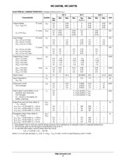
MAXIMUM RATINGS (Voltages Referenced to V
SS
)
Symbol Parameter Value Unit
V
DD
DC Supply Voltage Range −0.5 to +18.0 V
V
in
, V
out
Input or Output Voltage Range
(DC or Transient)
−0.5 to V
DD
+ 0.5 V
I
in
, I
out
Input or Output Current
(DC or Transient) per Pin
±10 mA
P
D
Power Dissipation, per Package
(Note 1)
500 mW
T
A
Ambient Temperature Range −55 to +125 °C
T
stg
Storage Temperature Range −65 to +150 °C
T
L
Lead Temperature
(8−Second Soldering)
260 °C
Maximum ratings are those values beyond which device damage can occur.
Maximum ratings applied to the device are individual stress limit values (not
normal operating conditions) and are not valid simultaneously. If these limits are
exceeded, device functional operation is not implied, damage may occur and
reliability may be affected.
1. Temperature Derating:
Plastic “P and D/DW” Packages: – 7.0 mW/C From 65C To 125C
This device contains protection circuitry to guard against damage due to high
static voltages or electric fields. However, precautions must be taken to avoid
applications of any voltage higher than maximum rated voltages to this
high−impedance circuit. For proper operation, V
in
and V
out
should be constrained
to the range V
SS
(V
in
or V
out
) V
DD
.
Unused inputs must always be tied to an appropriate logic voltage level
(e.g., either V
SS
or V
DD
). Unused outputs must be left open.
*For additional information on our Pb−Free strategy and soldering details, please
download the ON Semiconductor Soldering and Mounting Techniques
Reference Manual, SOLDERRM/D.
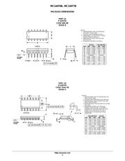
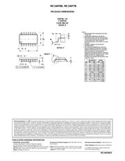
http://onsemi.com
MARKING
DIAGRAMS
1
14
PDIP−14
P SUFFIX
CASE 646
MC140xxBCP
AWLYYWW
SOIC−14
D SUFFIX
CASE 751A
1
14
140xxB
AWLYWW
xx = Specific Device Code
A = Assembly Location
WL, L = Wafer Lot
YY, Y = Year
WW, W = Work Week
SOEIAJ−14
F SUFFIX
CASE 965
1
14
MC140xxB
AWLYWW
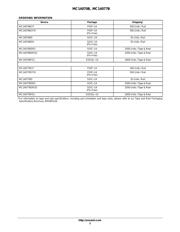
See detailed ordering and shipping information in the package
dimensions section on page 3 of this data sheet.
ORDERING INFORMATION
器件 Datasheet 文档搜索
AiEMA 数据库涵盖高达 72,405,303 个元件的数据手册,每天更新 5,000 多个 PDF 文件
