Datasheet 搜索 > 逻辑控制器 > ON Semiconductor(安森美) > MC14040BDR2 数据手册 > MC14040BDR2 其他数据使用手册 1/9 页
 器件3D模型
¥ 2.01
MC14040BDR2 其他数据使用手册 - ON Semiconductor(安森美)
制造商:
ON Semiconductor(安森美)
分类:
逻辑控制器
封装:
SOIC-16
描述:
12位二进制计数器 12−Bit Binary Counter
Pictures:
3D模型
符号图
焊盘图
引脚图
产品图
页面导航:
导航目录
MC14040BDR2数据手册
Page:
of 9 Go
若手册格式错乱,请下载阅览PDF原文件
© Semiconductor Components Industries, LLC, 2007
June, 2007 - Rev. 8
1 Publication Order Number:
MC14040B/D
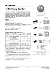
MC14040B
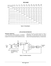
12-Bit Binary Counter
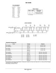
The MC14040B 12-stage binary counter is constructed with MOS
P-Channel and N-Channel enhancement mode devices in a single
monolithic structure. This part is designed with an input wave shaping
circuit and 12 stages of ripple-carry binary counter. The device
advances the count on the negative-going edge of the clock pulse.
Applications include time delay circuits, counter controls, and
frequency-driving circuits.
Features
•Fully Static Operation
•Diode Protection on All Inputs
•Supply Voltage Range = 3.0 Vdc to 18 Vdc
•Capable of Driving Two Low-power TTL Loads or One Low-power
Schottky TTL Load Over the Rated Temperature Range
•Common Reset Line
•Pin-for-Pin Replacement for CD4040B
•Pb-Free Packages are Available
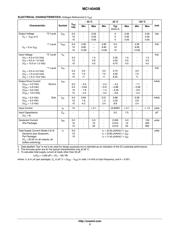
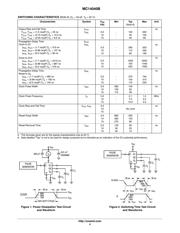
MAXIMUM RATINGS (Voltages Referenced to V
SS
)
Symbol
Parameter Value Unit
V
DD
DC Supply Voltage Range -0.5 to +18.0 V
V
in
, V
out
Input or Output Voltage Range
(DC or Transient)
-0.5 to V
DD
+ 0.5 V
I
in
, I
out
Input or Output Current
(DC or Transient) per Pin
±10 mA
P
D
Power Dissipation, per Package
(Note 1)
500 mW
T
A
Ambient Temperature Range -55 to +125 °C
T
stg
Storage Temperature Range -65 to +150 °C
T
L
Lead Temperature
(8-Second Soldering)
260 °C
Stresses exceeding Maximum Ratings may damage the device. Maximum
Ratings are stress ratings only. Functional operation above the Recommended
Operating Conditions is not implied. Extended exposure to stresses above the
Recommended Operating Conditions may affect device reliability.
1. Temperature Derating:
Plastic “P and D/DW” Packages: – 7.0 mW/_C From 65_C To 125_C
This device contains protection circuitry to guard against damage due to high
static voltages or electric fields. However, precautions must be taken to avoid
applications of any voltage higher than maximum rated voltages to this
high-impedance circuit. For proper operation, V
in
and V
out
should be constrained
to the range V
SS
v (V
in
or V
out
) v V
DD
.
Unused inputs must always be tied to an appropriate logic voltage level
(e.g., either V
SS
or V
DD
). Unused outputs must be left open.
http://onsemi.com
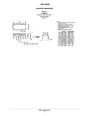
MARKING
DIAGRAMS
PDIP-16
P SUFFIX
CASE 648
MC14040BCP
AWLYYWWG
SOIC-16
D SUFFIX
CASE 751B
TSSOP-16
DT SUFFIX
CASE 948F
14040BG
AWLYWW
A = Assembly Location
WL, L = Wafer Lot
YY, Y = Year
WW, W = Work Week
G = Pb-Free Indicator
SOEIAJ-16
F SUFFIX
CASE 966
MC14040B
ALYWG
See detailed ordering and shipping information in the package
dimensions section on page 2 of this data sheet.
ORDERING INFORMATION
16
1
1
16
1
16
14
040B
ALYW G
G
1
16
器件 Datasheet 文档搜索
AiEMA 数据库涵盖高达 72,405,303 个元件的数据手册,每天更新 5,000 多个 PDF 文件
