Datasheet 搜索 > 逻辑控制器 > ON Semiconductor(安森美) > MC14050BCP 数据手册 > MC14050BCP 其他数据使用手册 1/8 页
 器件3D模型
¥ 0.792
MC14050BCP 其他数据使用手册 - ON Semiconductor(安森美)
制造商:
ON Semiconductor(安森美)
分类:
逻辑控制器
封装:
DIP
描述:
六角缓冲器 Hex Buffer
Pictures:
3D模型
符号图
焊盘图
引脚图
产品图
页面导航:
导航目录
MC14050BCP数据手册
Page:
of 8 Go
若手册格式错乱,请下载阅览PDF原文件
Semiconductor Components Industries, LLC, 2000
August, 2000 – Rev. 4
1 Publication Order Number:
MC14049B/D
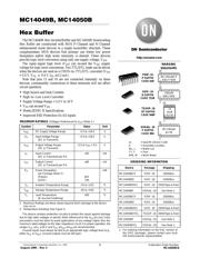
MC14049B, MC14050B
Hex Buffer
The MC14049B Hex Inverter/Buffer and MC14050B Noninverting
Hex Buffer are constructed with MOS P–Channel and N–Channel
enhancement mode devices in a single monolithic structure. These
complementary MOS devices find primary use where low power
dissipation and/or high noise immunity is desired. These devices
provide logic level conversion using only one supply voltage, V
DD
.
The input–signal high level (V
IH
) can exceed the V
DD
supply
voltage for logic level conversions. Two TTL/DTL loads can be driven
when the devices are used as a CMOS–to–TTL/DTL converter (V
DD
= 5.0 V, V
OL
0.4 V, I
OL
≥ 3.2 mA).
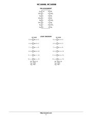
Note that pins 13 and 16 are not connected internally on these
devices; consequently connections to these terminals will not affect
circuit operation.
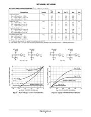
• High Source and Sink Currents
• High–to–Low Level Converter
• Supply Voltage Range = 3.0 V to 18 V
• V
IN
can exceed V
DD
• Meets JEDEC B Specifications
• Improved ESD Protection On All Inputs
MAXIMUM RATINGS (Voltages Referenced to V
SS
) (Note 2.)
Symbol
Parameter Value Unit
V
DD
DC Supply Voltage Range –0.5 to +18.0 V
V
in
Input Voltage Range
(DC or Transient)
–0.5 to +18.0 V
V
out
Output Voltage Range
(DC or Transient)
–0.5 to V
DD
+ 0.5 V
I
in
Input Current
(DC or Transient) per Pin
±10 mA
I
out
Output Current
(DC or Transient) per Pin
±45 mA
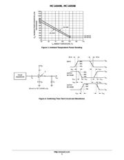
P
D
Power Dissipation,
per Package (Note 3.)
(Plastic)
(SOIC)
825
740
mW
T
A
Ambient Temperature Range –55 to +125 °C
T
stg
Storage Temperature Range –65 to +150 °C
T
L
Lead Temperature
(8–Second Soldering)
260 °C
2. Maximum Ratings are those values beyond which damage to the device
may occur.
3. Temperature Derating: See Figure 3.
This device contains protection circuitry to protect the inputs against damage
due to high static voltages or electric fields referenced to the V
SS
pin only. Extra
precautions must be taken to avoid applications of any voltage higher than the
maximum rated voltages to this high–impedance circuit. For proper operation, the
ranges V
SS
≤ V
in
≤ 18 V and V
SS
≤ V
out
≤ V
DD
are recommended.
Unused inputs must always be tied to an appropriate logic voltage level (e.g.,
either V
SS
or V
DD
). Unused outputs must be left open.
http://onsemi.com
xx = Specific Device Code
A = Assembly Location
WL, L = Wafer Lot
YY, Y = Year
WW, W = Work Week
Device Package Shipping
ORDERING INFORMATION
MC14049BCP PDIP–16 2000/Box
MC14049BD SOIC–16 2400/Box
MC14049BDR2 SOIC–16 2500/Tape & Reel
1. For ordering information on the EIAJ version of
the SOIC packages, please contact your local
ON Semiconductor representative.
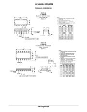
MARKING
DIAGRAMS
1
16
PDIP–16
P SUFFIX
CASE 648
MC140xxBCP
AWLYYWW
SOIC–16
D SUFFIX
CASE 751B
1
16
140xxB
AWLYWW
SOEIAJ–16
F SUFFIX
CASE 966
1
16
MC140xxB
ALYW
MC14049BF SOEIAJ–16 See Note 1.
MC14050BCP PDIP–16 2000/Box
MC14050BD SOIC–16 2400/Box
MC14050BDR2 SOIC–16 2500/Tape & Reel
MC14050BDTEL TSSOP–16 2000/Tape & Reel
MC14050BF SOEIAJ–16 See Note 1.
MC14050BFEL SOEIAJ–16 See Note 1.
TSSOP–16
DT SUFFIX
CASE 948F
14
0xxB
ALYW
1
16
器件 Datasheet 文档搜索
AiEMA 数据库涵盖高达 72,405,303 个元件的数据手册,每天更新 5,000 多个 PDF 文件
