Datasheet 搜索 > 接口芯片 > ON Semiconductor(安森美) > MC14052BDTR2G 数据手册 > MC14052BDTR2G 其他数据使用手册 1/12 页

 器件3D模型
¥ 1.351
MC14052BDTR2G 其他数据使用手册 - ON Semiconductor(安森美)
制造商:
ON Semiconductor(安森美)
分类:
接口芯片
封装:
TSSOP-16
描述:
4通道摸拟开关
Pictures:
3D模型
符号图
焊盘图
引脚图
产品图
页面导航:
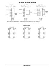
引脚图在P2Hot
典型应用电路图在P5
原理图在P5
封装尺寸在P10P11
焊盘布局在P10P11
型号编码规则在P1P9P12
标记信息在P1P11P12
封装信息在P9
技术参数、封装参数在P9
应用领域在P1P8P9
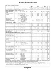
电气规格在P3P4
型号编号列表在P1
导航目录
MC14052BDTR2G数据手册
Page:
of 12 Go
若手册格式错乱,请下载阅览PDF原文件
© Semiconductor Components Industries, LLC, 2014
August, 2014 − Rev. 14
1 Publication Order Number:
MC14051B/D
MC14051B, MC14052B,
MC14053B
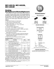
Analog
Multiplexers/Demultiplexers
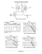
The MC14051B, MC14052B, and MC14053B analog multiplexers
are digitally−controlled analog switches. The MC14051B effectively
implements an SP8T solid state switch, the MC14052B a DP4T, and
the MC14053B a Triple SPDT. All three devices feature low ON
impedance and very low OFF leakage current. Control of analog
signals up to the complete supply voltage range can be achieved.
Features
• Triple Diode Protection on Control Inputs
• Switch Function is Break Before Make
• Supply Voltage Range = 3.0 Vdc to 18 Vdc
• Analog Voltage Range (V
DD
− V
EE
) = 3.0 to 18 V
Note: V
EE
must be ≤ V
SS
• Linearized Transfer Characteristics
• Low−noise − 12 nV/√Cycle, f ≥ 1.0 kHz Typical
• Pin−for−Pin Replacement for CD4051, CD4052, and CD4053
• For 4PDT Switch, See MC14551B
• For Lower R
ON
, Use the HC4051, HC4052, or HC4053
High−Speed CMOS Devices
• NLV Prefix for Automotive and Other Applications Requiring
Unique Site and Control Change Requirements; AEC−Q100
Qualified and PPAP Capable
• These Devices are Pb−Free and are RoHS Compliant
MAXIMUM RATINGS (Voltages Referenced to V
SS
)
Symbol Parameter Value Unit
V
DD
DC Supply Voltage Range
(Referenced to V
EE
, V
SS
≥ V
EE
)
−0.5 to +18.0 V
V
in
,
V
out
Input or Output Voltage Range
(DC or Transient) (Referenced to V
SS
for
Control Inputs and V
EE
for Switch I/O)
−0.5 to V
DD
+ 0.5 V
I
in
Input Current (DC or Transient)
per Control Pin
+10 mA
I
SW
Switch Through Current ±25 mA
P
D
Power Dissipation per Package (Note 1) 500 mW
T
A
Ambient Temperature Range −55 to +125 °C
T
stg
Storage Temperature Range −65 to +150 °C
T
L
Lead Temperature (8−Second Soldering) 260 °C
Stresses exceeding those listed in the Maximum Ratings table may damage the
device. If any of these limits are exceeded, device functionality should not be
assumed, damage may occur and reliability may be affected.
1. Temperature Derating: “D/DW” Packages: –7.0 mW/_C From 65_C To 125_C
This device contains protection circuitry to guard against damage due to high
static voltages or electric fields. However, precautions must be taken to avoid
applications of any voltage higher than maximum rated voltages to this
high−impedance circuit. For proper operation, V
in
and V
out
should be constrained to
the range V
SS
≤ (V
in
or V
out
) ≤ V
DD
.
Unused inputs must always be tied to an appropriate logic voltage level (e.g., either
V
SS
, V
EE
or V
DD
). Unused outputs must be left open.
http://onsemi.com
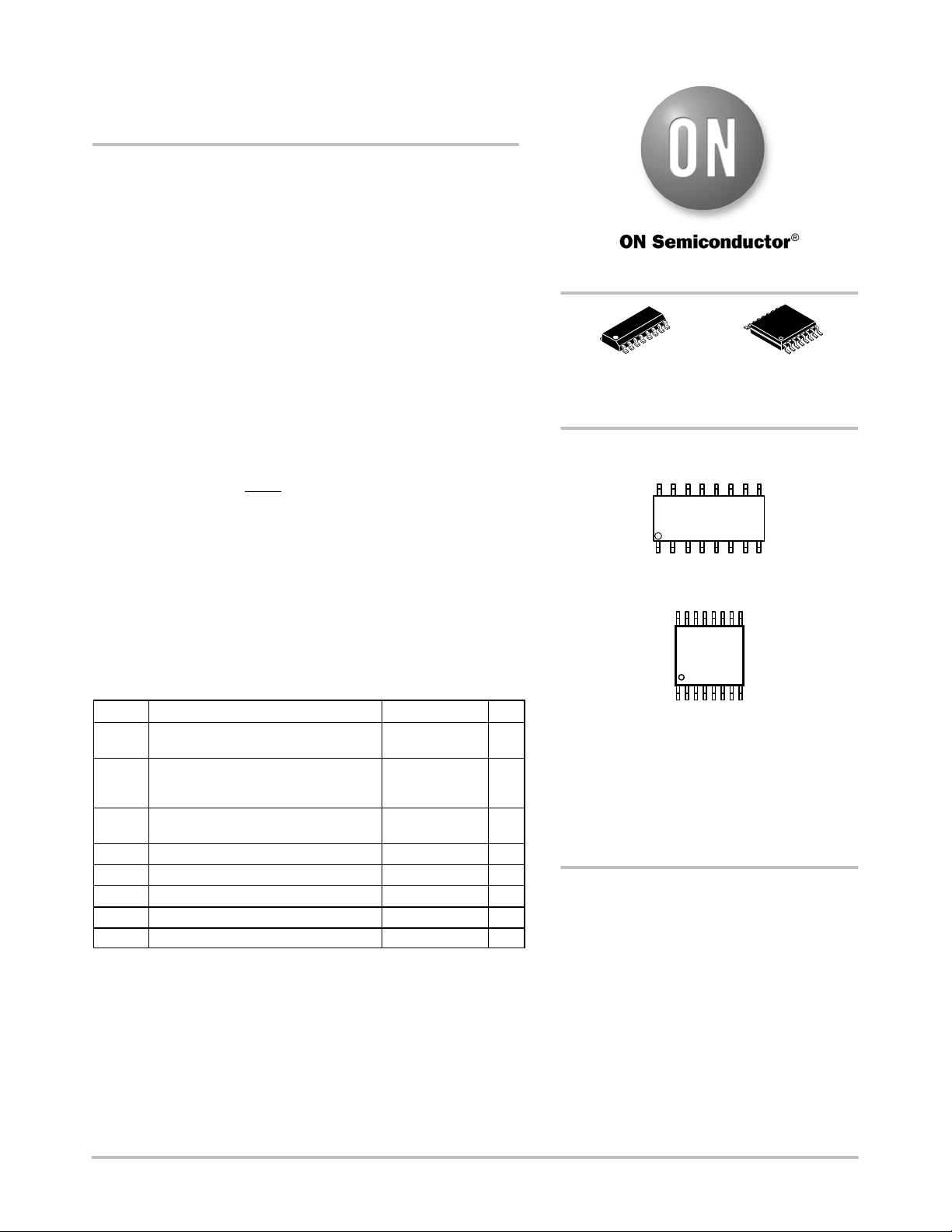
MARKING DIAGRAMS
SOIC−16
TSSOP−16
See detailed ordering and shipping information in the package
dimensions section on page 9 of this data sheet.
ORDERING INFORMATION
1405xBG
AWLYWW
14
05xB
ALYWG
G
1
1
16
1
1
16
x = 1, 2, or 3
A = Assembly Location
WL, L = Wafer Lot
Y = Year
WW, W = Work Week
G or G = Pb−Free Package
(Note: Microdot may be in either location)
SOIC−16
D SUFFIX
CASE 751B
TSSOP−16
DT SUFFIX
CASE 948F
器件 Datasheet 文档搜索
AiEMA 数据库涵盖高达 72,405,303 个元件的数据手册,每天更新 5,000 多个 PDF 文件
