Datasheet 搜索 > 移位寄存器 > ON Semiconductor(安森美) > MC14094BCP 数据手册 > MC14094BCP 其他数据使用手册 1/8 页
 器件3D模型
¥ 6.282
MC14094BCP 其他数据使用手册 - ON Semiconductor(安森美)
制造商:
ON Semiconductor(安森美)
分类:
移位寄存器
封装:
DIP-16
描述:
8级移位/存储寄存器具有三态输出 8−Stage Shift/Store Register with Three−State Outputs
Pictures:
3D模型
符号图
焊盘图
引脚图
产品图
页面导航:
导航目录
MC14094BCP数据手册
Page:
of 8 Go
若手册格式错乱,请下载阅览PDF原文件
Semiconductor Components Industries, LLC, 2000
AUGUST, 2000 – Rev. 4
1 Publication Order Number:
MC14094B/D
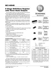
MC14094B
8-Stage Shift/Store Register
with Three-State Outputs
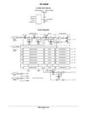
The MC14094B combines an 8–stage shift register with a data latch
for each stage and a three–state output from each latch.
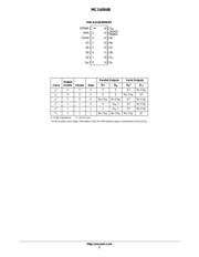
Data is shifted on the positive clock transition and is shifted from the
seventh stage to two serial outputs. The Q
S
output data is for use in
high–speed cascaded systems. The Q′
S
output data is shifted on the
following negative clock transition for use in low–speed cascaded
systems.
Data from each stage of the shift register is latched on the negative
transition of the strobe input. Data propagates through the latch while
strobe is high.
Outputs of the eight data latches are controlled by three–state
buffers which are placed in the high–impedance state by a logic Low
on Output Enable.
• Three–State Outputs
• Capable of Driving Two Low–Power TTL Loads or One Low–Power
Schottky TTL Load Over the Rated Temperature Range
• Input Diode Protection
• Data Latch
• Dual Outputs for Data Out on Both Positive and
Negative Clock Transitions
• Useful for Serial–to–Parallel Data Conversion
• Pin–for–Pin Compatible with CD4094B
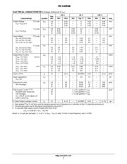
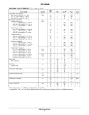
MAXIMUM RATINGS (Voltages Referenced to V
SS
) (Note 2.)
Symbol
Parameter Value Unit
V
DD
DC Supply Voltage Range –0.5 to +18.0 V
V
in
, V
out
Input or Output Voltage Range
(DC or Transient)
–0.5 to V
DD
+ 0.5 V
I
in
, I
out
Input or Output Current
(DC or Transient) per Pin
±10 mA
P
D
Power Dissipation,
per Package (Note 3.)
500 mW
T
A
Ambient Temperature Range –55 to +125 °C
T
stg
Storage Temperature Range –65 to +150 °C
T
L
Lead Temperature
(8–Second Soldering)
260 °C
2. Maximum Ratings are those values beyond which damage to the device
may occur.
3. Temperature Derating:
Plastic “P and D/DW” Packages: – 7.0 mW/C From 65C To 125C
This device contains protection circuitry to guard against damage due to high
static voltages or electric fields. However, precautions must be taken to avoid
applications of any voltage higher than maximum rated voltages to this
high–impedance circuit. For proper operation, V
in
and V
out
should be constrained
to the range V
SS
(V
in
or V
out
) V
DD
.
Unused inputs must always be tied to an appropriate logic voltage level (e.g.,
either V
SS
or V
DD
). Unused outputs must be left open.
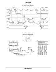
Device Package Shipping
ORDERING INFORMATION
MC14094BCP PDIP–16 2000/Box
MC14094BD SOIC–16
http://onsemi.com
48/Rail
MC14094BDR2 SOIC–16 2500/Tape & Reel
MC14094BDT TSSOP–16 96/Rail
MC14094BDTR2 TSSOP–16
2500/Tape & Reel
MARKING
DIAGRAMS
1
16
PDIP–16
P SUFFIX
CASE 648
MC14094BCP
AWLYYWW
SOIC–16
D SUFFIX
CASE 751B
TSSOP–16
DT SUFFIX
CASE 948F
1
16
14094B
AWLYWW
14
094B
ALYW
1
16
A = Assembly Location
WL, L = Wafer Lot
YY, Y = Year
WW, W = Work Week
SOEIAJ–16
F SUFFIX
CASE 966
1
16
MC14094B
ALYW
MC14094BF SOEIAJ–16 See Note 1.
1. For ordering information on the EIAJ version of the
SOIC packages, please contact your local ON
Semiconductor representative.
器件 Datasheet 文档搜索
AiEMA 数据库涵盖高达 72,405,303 个元件的数据手册,每天更新 5,000 多个 PDF 文件
