Datasheet 搜索 > 计数器 > ON Semiconductor(安森美) > MC14516BFEL 数据手册 > MC14516BFEL 其他数据使用手册 1/11 页

¥ 0
MC14516BFEL 其他数据使用手册 - ON Semiconductor(安森美)
制造商:
ON Semiconductor(安森美)
分类:
计数器
封装:
SOEIAJ-16
描述:
二进制加/减计数器 Binary Up/Down Counter
Pictures:
3D模型
符号图
焊盘图
引脚图
产品图
页面导航:
导航目录
MC14516BFEL数据手册
Page:
of 11 Go
若手册格式错乱,请下载阅览PDF原文件
© Semiconductor Components Industries, LLC, 2006
June, 2006 − Rev. 7
1 Publication Order Number:
MC14516B/D
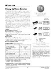
MC14516B
Binary Up/Down Counter
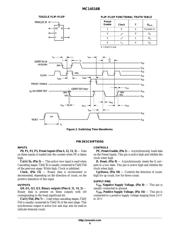
The MC14516B synchronous up/down binary counter is
constructed with MOS P−channel and N−channel enhancement mode
devices in a monolithic structure.
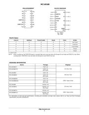
This counter can be preset by applying the desired value, in binary,
to the Preset inputs (P0, P1, P2, P3) and then bringing the Preset
Enable (PE) high. The direction of counting is controlled by applying
a high (for up counting) or a low (for down counting) to the
UP/DOWN input. The state of the counter changes on the positive
transition of the clock input.
Cascading can be accomplished by connecting the Carry Out to the
Carry In of the next stage while clocking each counter in parallel. The
outputs (Q0, Q1, Q2, Q3) can be reset to a low state by applying a high
to the reset (R) pin.
This CMOS counter finds primary use in up/down and difference
counting. Other applications include: (1) Frequency synthesizer
applications where low power dissipation and/or high noise immunity
is desired, (2) Analog−to−Digital and Digital−to−Analog conversions,
and (3) Magnitude and sign generation.
Features
• Diode Protection on All Inputs
• Supply Voltage Range = 3.0 Vdc to 18 Vdc
• Internally Synchronous for High Speed
• Logic Edge−Clocked Design — Count Occurs on Positive Going
Edge of Clock
• Single Pin Reset
• Asynchronous Preset Enable Operation
• Capable of Driving Two Low−Power TTL Loads or One Low−Power
Schottky Load Over the Rated Temperature Range
• Pb−Free Packages are Available*
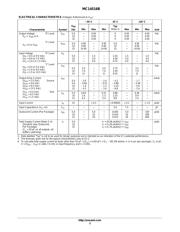
MAXIMUM RATINGS (Voltages Referenced to V
SS
)
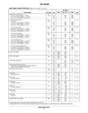
Parameter Symbol Value Unit
DC Supply Voltage Range V
DD
−0.5 to +18.0 V
Input or Output Voltage Range
(DC or Transient)
V
in
, V
out
−0.5 to V
DD
+ 0.5
V
Input or Output Current (DC or Transient)
per Pin
I
in
, I
out
± 10 mA
Power Dissipation, per Package (Note 1) P
D
500 mW
Ambient Temperature Range T
A
−55 to +125 °C
Storage Temperature Range T
stg
−65 to +150 °C
Lead Temperature (8−Second Soldering) T
L
260 °C
Stresses exceeding Maximum Ratings may damage the device. Maximum
Ratings are stress ratings only. Functional operation above the Recommended
Operating Conditions is not implied. Extended exposure to stresses above the
Recommended Operating Conditions may affect device reliability.
1. Temperature Derating: Plastic “P and D/DW”
Packages: – 7.0 mW/_C From 65_C To 125_C
*For additional information on our Pb−Free strategy and soldering details, please
download the ON Semiconductor Soldering and Mounting Techniques
Reference Manual, SOLDERRM/D.
This device contains protection circuitry to guar
d
a
gainst damage due to high static voltages or electr
ic
f
ields. However, precautions must be taken to avo
id
a
pplications of any voltage higher than maximum rate
d
v
oltages to this high−impedance circuit. For prope
r
o
peration, V
in
and V
out
should be constrained to th
e
r
ange V
SS
v (V
in
or V
out
) v V
DD
.
Unused inputs must always be tied to an appropria
te
l
ogic voltage level (e.g., either V
SS
or V
DD
). Unuse
d
o
utputs must be left open.
http://onsemi.com
See detailed ordering and shipping information in the package
dimensions section on page 2 of this data sheet.
ORDERING INFORMATION
A = Assembly Location
WL, L = Wafer Lot
YY, Y = Year
WW, W = Work Week
G = Pb−Free Package
MARKING
DIAGRAMS
PDIP−16
P SUFFIX
CASE 648
SOIC−16
D SUFFIX
CASE 751B
1
16
14516BG
AWLYWW
SOEIAJ−16
F SUFFIX
CASE 966
1
16
MC14516B
ALYWG
16
1
MC14516BCP
AWLYYWWG
1
1
1
器件 Datasheet 文档搜索
AiEMA 数据库涵盖高达 72,405,303 个元件的数据手册,每天更新 5,000 多个 PDF 文件
