Datasheet 搜索 > 逻辑控制器 > ON Semiconductor(安森美) > MC14521BCPG 数据手册 > MC14521BCPG 其他数据使用手册 1/12 页
 器件3D模型
¥ 3.438
MC14521BCPG 其他数据使用手册 - ON Semiconductor(安森美)
制造商:
ON Semiconductor(安森美)
分类:
逻辑控制器
封装:
DIP-16
描述:
24级分频器
Pictures:
3D模型
符号图
焊盘图
引脚图
产品图
页面导航:
导航目录
MC14521BCPG数据手册
Page:
of 12 Go
若手册格式错乱,请下载阅览PDF原文件
Semiconductor Components Industries, LLC, 2000
August, 2000 – Rev. 4
1 Publication Order Number:
MC14521B/D
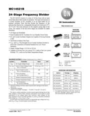
MC14521B
24-Stage Frequency Divider
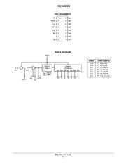
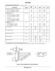
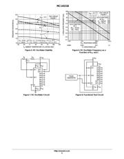
The MC14521B consists of a chain of 24 flip–flops with an input
circuit that allows three modes of operation. The input will function as
a crystal oscillator, an RC oscillator, or as an input buffer for an
external oscillator. Each flip–flop divides the frequency of the
previous flip–flop by two, consequently this part will count up to 2
24
=
16,777,216. The count advances on the negative going edge of the
clock. The outputs of the last seven–stages are available for added
flexibility.
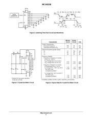
• All Stages are Resettable
• Reset Disables the RC Oscillator for Low Standby Power Drain
• RC and Crystal Oscillator Outputs Are Capable of Driving External
Loads
• Test Mode to Reduce Test Time
• V
DD
′ and V
SS
′ Pins Brought Out on Crystal Oscillator Inverter to
Allow the Connection of External Resistors for Low–Power
Operation
• Supply Voltage Range = 3.0 Vdc to 18 Vdc
• Capable of Driving Two Low–power TTL Loads or One Low–power
Schottky TTL Load over the Rated Temperature Range.
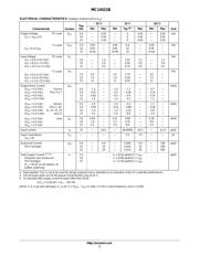
MAXIMUM RATINGS (Voltages Referenced to V
SS
) (Note 2.)
Symbol Parameter Value Unit
V
DD
DC Supply Voltage Range –0.5 to +18.0 V
V
in
, V
out
Input or Output Voltage Range
(DC or Transient)
–0.5 to V
DD
+ 0.5 V
I
in
, I
out
Input or Output Current
(DC or Transient) per Pin
±10 mA
P
D
Power Dissipation,
per Package (Note 3.)
500 mW
T
A
Ambient Temperature Range –55 to +125 °C
T
stg
Storage Temperature Range –65 to +150 °C
T
L
Lead Temperature
(8–Second Soldering)
260 °C
2. Maximum Ratings are those values beyond which damage to the device
may occur.
3. Temperature Derating:
Plastic “P and D/DW” Packages: – 7.0 mW/C From 65C To 125C
This device contains protection circuitry to guard against damage due to high
static voltages or electric fields. However, precautions must be taken to avoid
applications of any voltage higher than maximum rated voltages to this
high–impedance circuit. For proper operation, V
in
and V
out
should be constrained
to the range V
SS
(V
in
or V
out
) V
DD
.
Unused inputs must always be tied to an appropriate logic voltage level (e.g.,
either V
SS
or V
DD
). Unused outputs must be left open.
http://onsemi.com
A = Assembly Location
WL, L = Wafer Lot
YY, Y = Year
WW, W = Work Week
Device Package Shipping
ORDERING INFORMATION
MC14521BCP PDIP–16 2000/Box
MC14521BD SOIC–16 48/Rail
MC14521BDR2 SOIC–16 2500/Tape & Reel
1. For ordering information on the EIAJ version of
the SOIC packages, please contact your local
ON Semiconductor representative.
MARKING
DIAGRAMS
1
16
PDIP–16
P SUFFIX
CASE 648
MC14521BCP
AWLYYWW
SOIC–16
D SUFFIX
CASE 751B
1
16
14521B
AWLYWW
SOEIAJ–16
F SUFFIX
CASE 966
1
16
MC14521B
ALYW
MC14521BFEL SOEIAJ–16 See Note 1.
MC14521BFR2 SOEIAJ–16 See Note 1.
MC14521BF SOEIAJ–16 See Note 1.
器件 Datasheet 文档搜索
AiEMA 数据库涵盖高达 72,405,303 个元件的数据手册,每天更新 5,000 多个 PDF 文件
