Datasheet 搜索 > 主动器件 > ON Semiconductor(安森美) > MC14541BCP 数据手册 > MC14541BCP 其他数据使用手册 1/12 页
 器件3D模型
¥ 0
MC14541BCP 其他数据使用手册 - ON Semiconductor(安森美)
制造商:
ON Semiconductor(安森美)
分类:
主动器件
封装:
PDIP
描述:
可编程定时器 Programmable Timer
Pictures:
3D模型
符号图
焊盘图
引脚图
产品图
页面导航:
导航目录
MC14541BCP数据手册
Page:
of 12 Go
若手册格式错乱,请下载阅览PDF原文件
Semiconductor Components Industries, LLC, 2002
April, 2002 – Rev. 5
1 Publication Order Number:
MC14528B/D
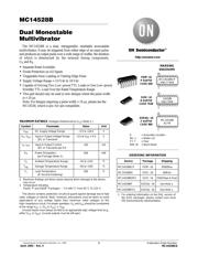
MC14528B
Dual Monostable
Multivibrator
The MC14528B is a dual, retriggerable, resettable monostable
multivibrator. It may be triggered from either edge of an input pulse,
and produces an output pulse over a wide range of widths, the duration
of which is determined by the external timing components,
C
X
and R
X
.
• Separate Reset Available
• Diode Protection on All Inputs
• Triggerable from Leading or Trailing Edge Pulse
• Supply Voltage Range = 3.0 Vdc to 18 Vdc
• Capable of Driving Two Low–power TTL Loads or One Low–power
Schottky TTL Load Over the Rated Temperature Range
• This part should only be used in new designs where the pulse width
is < 10 s.
Note: For designs requiring a pulse width > 10 s, please see the
MC14538, which is pin–for–pin compatible.
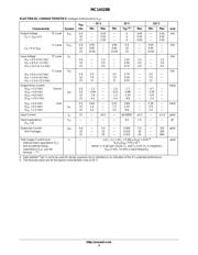
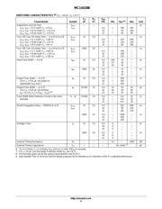
MAXIMUM RATINGS (Voltages Referenced to V
SS
) (Note 2.)
Symbol
Parameter Value Unit
V
DD
DC Supply Voltage Range –0.5 to +18.0 V
V
in
, V
out
Input or Output Voltage Range
(DC or Transient)
–0.5 to V
DD
+ 0.5 V
I
in
, I
out
Input or Output Current
(DC or Transient) per Pin
±10 mA
P
D
Power Dissipation,
per Package (Note 3.)
500 mW
T
A
Ambient Temperature Range –55 to +125 °C
T
stg
Storage Temperature Range –65 to +150 °C
T
L
Lead Temperature
(8–Second Soldering)
260 °C
2. Maximum Ratings are those values beyond which damage to the device
may occur.
3. Temperature Derating:
Plastic “P and D/DW” Packages: – 7.0 mW/C From 65C To 125C
This device contains protection circuitry to guard against damage due to high
static voltages or electric fields. However, precautions must be taken to avoid
applications of any voltage higher than maximum rated voltages to this
high–impedance circuit. For proper operation, V
in
and V
out
should be constrained
to the range V
SS
(V
in
or V
out
) V
DD
.
Unused inputs must always be tied to an appropriate logic voltage level (e.g.,
either V
SS
or V
DD
). Unused outputs must be left open.
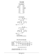
A = Assembly Location
WL, L = Wafer Lot
YY, Y = Year
WW, W = Work Week
Device Package Shipping
ORDERING INFORMATION
MC14528BCP PDIP–16 2000/Box
MC14528BD SOIC–16 48/Rail
MC14528BDR2 SOIC–16 2500/Tape & Reel
1. For ordering information on the EIAJ version of
the SOIC packages, please contact your local
ON Semiconductor representative.
MARKING
DIAGRAMS
1
16
PDIP–16
P SUFFIX
CASE 648
MC14528BCP
AWLYYWW
SOIC–16
D SUFFIX
CASE 751B
1
16
14528B
AWLYWW
SOEIAJ–16
F SUFFIX
CASE 966
1
16
MC14528B
ALYW
MC14528BFEL SOEIAJ–16 See Note 1.
MC14528BF SOEIAJ–16 See Note 1.
http://onsemi.com
器件 Datasheet 文档搜索
AiEMA 数据库涵盖高达 72,405,303 个元件的数据手册,每天更新 5,000 多个 PDF 文件
