Datasheet 搜索 > 可编程定时器芯片 > ON Semiconductor(安森美) > MC14541BDR2 数据手册 > MC14541BDR2 产品手册 1/8 页
 器件3D模型
¥ 0.461
MC14541BDR2 产品手册 - ON Semiconductor(安森美)
制造商:
ON Semiconductor(安森美)
分类:
可编程定时器芯片
封装:
SOIC-14
描述:
可编程定时器 Programmable Timer
Pictures:
3D模型
符号图
焊盘图
引脚图
产品图
页面导航:
导航目录
MC14541BDR2数据手册
Page:
of 8 Go
若手册格式错乱,请下载阅览PDF原文件
Semiconductor Components Industries, LLC, 2000
March, 2000 – Rev. 6
1 Publication Order Number:
MC14541B/D
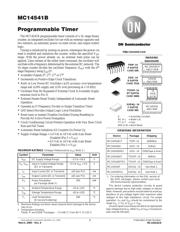
MC14541B
Pr ogrammable Timer
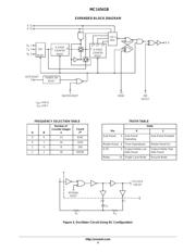
The MC14541B programmable timer consists of a 16–stage binary
counter, an integrated oscillator for use with an external capacitor and
two resistors, an automatic power–on reset circuit, and output control
logic.
Timing is initialized by turning on power, whereupon the power–on
reset is enabled and initializes the counter, within the specified V
DD
range. With the power already on, an external reset pulse can be
applied. Upon release of the initial reset command, the oscillator will
oscillate with a frequency determined by the external RC network. The
16–stage counter divides the oscillator frequency (f
osc
) with the n
th
stage frequency being f
osc
/2
n
.
• Available Outputs 2
8
, 2
10
, 2
13
or 2
16
• Increments on Positive Edge Clock Transitions
• Built–in Low Power RC Oscillator (± 2% accuracy over temperature
range and ± 20% supply and ± 3% over processing at < 10 kHz)
• Oscillator May Be Bypassed if External Clock Is Available (Apply
external clock to Pin 3)
• External Master Reset Totally Independent of Automatic Reset
Operation
• Operates as 2
n
Frequency Divider or Single Transition Timer
• Q/Q Select Provides Output Logic Level Flexibility
• Reset (auto or master) Disables Oscillator During Resetting to
Provide No Active Power Dissipation
• Clock Conditioning Circuit Permits Operation with Very Slow Clock
Rise and Fall Times
• Automatic Reset Initializes All Counters On Power Up
• Supply Voltage Range = 3.0 Vdc to 18 Vdc with Auto Reset
Supply Voltage Range = Disabled (Pin 5 = V
DD
)
Supply Voltage Range = 8.5 Vdc to 18 Vdc with Auto Reset
Supply Voltage Range = Enabled (Pin 5 = V
SS
)
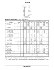
MAXIMUM RATINGS (Voltages Referenced to V
SS
) (Note 2.)
Symbol
Parameter Value Unit
V
DD
DC Supply Voltage Range –0.5 to +18.0 V
V
in
, V
out
Input or Output Voltage Range
(DC or Transient)
–0.5 to V
DD
+ 0.5 V
I
in
Input Current (DC or Transient) ±10 (per Pin) mA
I
out
Output Current (DC or Transient) ±45 (per Pin) mA
P
D
Power Dissipation,
per Package (Note 3.)
500 mW
T
A
Ambient Temperature Range –55 to +125 °C
T
stg
Storage Temperature Range –65 to +150 °C
T
L
Lead Temperature
(8–Second Soldering)
260 °C
2. Maximum Ratings are those values beyond which damage to the device
may occur.
3. Temperature Derating:
Plastic “P and D/DW” Packages: – 7.0 mW/
_
C From 65
_
C To 125
_
C
http://onsemi.com
A = Assembly Location
WL or L = Wafer Lot
YY or Y = Year
WW or W = Work Week
Device Package Shipping
ORDERING INFORMATION
MC14541BCP PDIP–14 2000/Box
MC14541BD SOIC–14 55/Rail
MC14541BDR2 SOIC–14 2500/Tape & Reel
1. For ordering information on the EIAJ version of
the SOIC packages, please contact your local
ON Semiconductor representative.
MC14541BDTR2 TSSOP–14 2500/Tape & Reel
MC14541BDT TSSOP–14 96/Rail
MC14541BF SOEIAJ–14 See Note 1.
This device contains protection circuitry to guard
against damage due to high static voltages or electric
fields. However, precautions must be taken to avoid ap-
plications of any voltage higher than maximum rated
voltages to this high–impedance circuit. For proper
operation, V
in
and V
out
should be constrained to the
range V
SS
v
(V
in
or V
out
)
v
V
DD
.
Unused inputs must always be tied to an appropriate
logic voltage level (e.g., either V
SS
or V
DD
). Unused out-
puts must be left open.
MC14541BFEL SOEIAJ–14 See Note 1.
MARKING
DIAGRAMS
1
14
PDIP–14
P SUFFIX
CASE 646
MC14541BCP
AWLYYWW
SOIC–14
D SUFFIX
CASE 751A
TSSOP–14
DT SUFFIX
CASE 948G
1
14
14541B
AWLYWW
14
541B
ALYW
1
14
SOEIAJ–14
F SUFFIX
CASE 965
1
14
MC14541B
AWLYWW
器件 Datasheet 文档搜索
AiEMA 数据库涵盖高达 72,405,303 个元件的数据手册,每天更新 5,000 多个 PDF 文件
