Datasheet 搜索 > 计数器 > ON Semiconductor(安森美) > MC14569BCP 数据手册 > MC14569BCP 其他数据使用手册 3/14 页
 器件3D模型
¥ 0
MC14569BCP 其他数据使用手册 - ON Semiconductor(安森美)
制造商:
ON Semiconductor(安森美)
分类:
计数器
封装:
PDIP-16
描述:
可编程分频-N双4位二进制/ BCD减计数器 Programmable Divide-By-N Dual 4-Bit Binary/BCD Down Counter
Pictures:
3D模型
符号图
焊盘图
引脚图
产品图
页面导航:
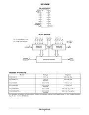
引脚图在P2P5Hot
典型应用电路图在P10P11
原理图在P2
封装尺寸在P12P13
型号编码规则在P1P2P14
标记信息在P1
封装信息在P2
技术参数、封装参数在P2
应用领域在P1P11
电气规格在P3
导航目录
MC14569BCP数据手册
Page:
of 14 Go
若手册格式错乱,请下载阅览PDF原文件
MC14569B
http://onsemi.com
3
ÎÎÎÎÎÎÎÎÎÎÎÎÎÎÎÎÎÎÎÎÎÎÎÎÎÎÎÎÎÎÎÎÎ
ÎÎÎÎÎÎÎÎÎÎÎÎÎÎÎÎÎÎÎÎÎÎÎÎÎÎÎÎÎÎÎÎÎ
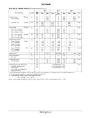
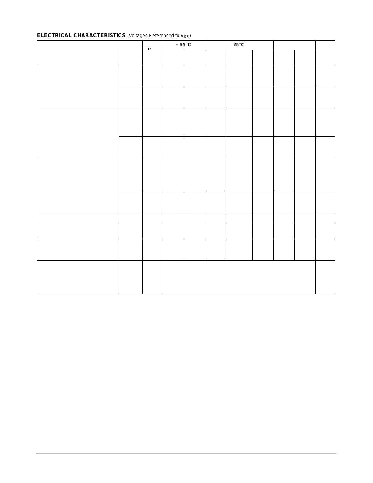
ELECTRICAL CHARACTERISTICS (Voltages Referenced to V
SS
)
V
– 55C 25C 125C
Characteristic Symbol
V
DD
Vdc
Min Max Min Typ
(Note 2)
Max Min Max
Unit
Output Voltage “0” Level
V
in
= V
DD
or 0
V
OL
5.0
10
15
−
−
−
0.05
0.05
0.05
−
−
−
0
0
0
0.05
0.05
0.05
−
−
−
0.05
0.05
0.05
Vdc
V
in
= 0 or V
DD
“1” Level V
OH
5.0
10
15
4.95
9.95
14.95
−
−
−
4.95
9.95
14.95
5.0
10
15
−
−
−
4.95
9.95
14.95
−
−
−
Vdc
Input Voltage “0” Level
(V
O
= 4.5 or 0.5 Vdc)
(V
O
= 9.0 or 1.0 Vdc)
(V
O
= 13.5 or 1.5 Vdc)
V
IL
5.0
10
15
−
−
−
1.5
3.0
4.0
−
−
−
2.25
4.50
6.75
1.5
3.0
4.0
−
−
−
1.5
3.0
4.0
Vdc
(V
O
= 0.5 or 4.5 Vdc) “1” Level
(V
O
= 1.0 or 9.0 Vdc)
(V
O
= 1.5 or 13.5 Vdc)
V
IH
5.0
10
15
3.5
7.0
11
−
−
−
3.5
7.0
11
2.75
5.50
8.25
−
−
−
3.5
7.0
11
−
−
−
Vdc
Output Drive Current
(V
OH
= 2.5 Vdc) Source
(V
OH
= 4.6 Vdc)
(V
OH
= 9.5 Vdc)
(V
OH
= 13.5 Vdc)
I
OH
5.0
5.0
10
15
– 3.0
– 0.64
– 1.6
– 4.2
−
−
−
−
– 2.4
– 0.51
– 1.3
– 3.4
– 4.2
– 0.88
– 2.25
– 8.8
−
−
−
−
– 1.7
– 0.36
– 0.9
– 2.4
−
−
−
−
mAdc
(V
OL
= 0.4 Vdc) Sink
(V
OL
= 0.5 Vdc)
(V
OL
= 1.5 Vdc)
I
OL
5.0
10
15
0.64
1.6
4.2
−
−
−
0.51
1.3
3.4
0.88
2.25
8.8
−
−
−
0.36
0.9
2.4
−
−
−
mAdc
Input Current I
in
15 − ±0.1 − ±0.00001 ±0.1 − ±1.0 Adc
Input Capacitance
(V
in
= 0)
C
in
− − − − 5.0 7.5 − − pF
Quiescent Current
(Per Package)
I
DD
5.0
10
15
−
−
−
5.0
10
20
−
−
−
0.005
0.010
0.015
5.0
10
20
−
−
−
150
300
600
Adc
Total Supply Current (Notes 3 & 4)
(Dynamic plus Quiescent,
Per Package)
(C
L
= 50 pF on all outputs, all
buffers switching)
I
T
5.0
10
15
I
T
= (0.58 A/kHz) f + I
DD
I
T
= (1.20 A/kHz) f + I
DD
I
T
= (1.95 A/kHz) f + I
DD
Adc
2. Data labelled “Typ” is not to be used for design purposes but is intended as an indication of the IC’s potential performance.
3. The formulas given are for the typical characteristics only at 25C.
4. To calculate total supply current at loads other than 50 pF:
I
T
(C
L
) = I
T
(50 pF) + (C
L
– 50) Vfk
where: I
T
is in A (per package), C
L
in pF, V = (V
DD
– V
SS
) in volts, f in kHz is input frequency, and k = 0.001.
器件 Datasheet 文档搜索
AiEMA 数据库涵盖高达 72,405,303 个元件的数据手册,每天更新 5,000 多个 PDF 文件
