Datasheet 搜索 > 逻辑芯片 > ON Semiconductor(安森美) > MC14584BDR2 数据手册 > MC14584BDR2 其他数据使用手册 1/13 页

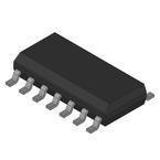
 器件3D模型
¥ 1.436
MC14584BDR2 其他数据使用手册 - ON Semiconductor(安森美)
制造商:
ON Semiconductor(安森美)
分类:
逻辑芯片
封装:
SOIC-14
描述:
六角施密特触发器 Hex Schmitt Trigger
Pictures:
3D模型
符号图
焊盘图
引脚图
产品图
页面导航:
功能描述在P1
导航目录
MC14584BDR2数据手册
Page:
of 13 Go
若手册格式错乱,请下载阅览PDF原文件

Issue Date: 02-Dec-2008 Rev.07-31-07 Page 1 of 13
INITIAL PRODUCT/PROCESS CHANGE NOTIFICATION
Generic Copy
02-Dec-2008
SUBJECT: ON Semiconductor Initial Product/Process Change Notification #16177
TITLE: Initial Notification for Transfer of Standard Logic Metal Gate Integrated Circuits Die
Manufacturing From ON Semiconductor Piestany (Slovakia) To ON Semiconductor Roznov (Czeck
Republic).
PROPOSED FIRST SHIP DATE: 02-Apr-2009
AFFECTED CHANGE CATEGORY: ON Semiconductor Fab Site
AFFECTED PRODUCT DIVISION: Standard Logic Products
FOR ANY QUESTIONS CONCERNING THIS NOTIFICATION:
Contact your local ON Semiconductor Sales Office or Won Kang <Won.Kang@onsemi.com
>
NOTIFICATION TYPE:
Initial Product/Process Change Notification (IPCN)
First change notification sent to customers. IPCNs are issued at least 120 days prior to implementation
of the change. An IPCN is advance notification about an upcoming change and contains general
information regarding the change details and devices affected. It also contains the preliminary
reliability qualification plan.
The completed qualification and characterization data will be included in the Final Product/Process
Change Notification (FPCN).
This IPCN notification will be followed by a Final Product/Process Change Notification (FPCN) at
least 90 days prior to implementation of the change.
DESCRIPTION AND PURPOSE:
May 14, 2008 - ON Semiconductor (Nasdaq: ONNN), has announced plans to close its two
wafer manufacturing facilities located in Piestany, Slovakia, and transfer the production lines
to other company-owned facilities. The targeted close date is Q4 2009.
Description of the change:
The transfer and qualification of the Metal Gate CMOS process and the associated integrated
circuits from the ON Semiconductor Piestany facility (Slovakia) to the Roznov CZ4 wafer
fabrication site located in the Czeck Republic.
The Roznov CZ4 site is certified according to ISO/TS16949 standard.
The Metal Gate process is a CMOS technology being replicated at Roznov CZ4 to get the
same electrical and reliability performances as the Piestany wafer fab.
器件 Datasheet 文档搜索
AiEMA 数据库涵盖高达 72,405,303 个元件的数据手册,每天更新 5,000 多个 PDF 文件


