Datasheet 搜索 > 放大器、缓冲器 > ON Semiconductor(安森美) > MC33074DR2 数据手册 > MC33074DR2 其他数据使用手册 1/27 页
 器件3D模型
¥ 0
MC33074DR2 其他数据使用手册 - ON Semiconductor(安森美)
制造商:
ON Semiconductor(安森美)
分类:
放大器、缓冲器
封装:
SOIC-14
描述:
高压摆率,宽带宽,单电源运算放大器 High Slew Rate, Wide Bandwidth, Single Supply Operational Amplifiers
Pictures:
3D模型
符号图
焊盘图
引脚图
产品图
页面导航:
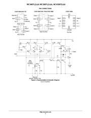
引脚图在P2Hot
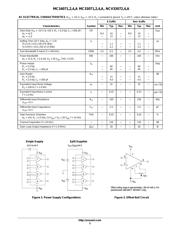
原理图在P2
封装尺寸在P22P23P24P25P26
焊盘布局在P23P24P25P26
型号编码规则在P1P18P19P20P26
标记信息在P1P21P26
封装信息在P19P20
技术参数、封装参数在P19P20
应用领域在P1P11P13P16
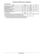
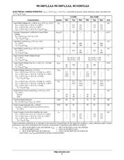
电气规格在P4P5
型号编号列表在P3
导航目录
MC33074DR2数据手册
Page:
of 27 Go
若手册格式错乱,请下载阅览PDF原文件
© Semiconductor Components Industries, LLC, 2013
December, 2013 − Rev. 21
1 Publication Order Number:
MC34071/D
MC34071,2,4,A
MC33071,2,4,A,
NCV33072,4,A
Single Supply 3.0 V to 44 V
Operational Amplifiers
Quality bipolar fabrication with innovative design concepts are
employed for the MC33071/72/74, MC34071/72/74, NCV33072/74A
series of monolithic operational amplifiers. This series of operational
amplifiers offer 4.5 MHz of gain bandwidth product, 13 V/ms slew rate
and fast settling time without the use of JFET device technology.
Although this series can be operated from split supplies, it is
particularly suited for single supply operation, since the common
mode input voltage range includes ground potential (V
EE
). With a
Darlington input stage, this series exhibits high input resistance, low
input offset voltage and high gain. The all NPN output stage,
characterized by no deadband crossover distortion and large output
voltage swing, provides high capacitance drive capability, excellent
phase and gain margins, low open loop high frequency output
impedance and symmetrical source/sink AC frequency response.
The MC33071/72/74, MC34071/72/74, NCV33072/74,A series of
devices are available in standard or prime performance (A Suffix)
grades and are specified over the commercial, industrial/vehicular or
military temperature ranges. The complete series of single, dual and
quad operational amplifiers are available in plastic DIP, SOIC, QFN
and TSSOP surface mount packages.
Features
• Wide Bandwidth: 4.5 MHz
• High Slew Rate: 13 V/ms
• Fast Settling Time: 1.1 ms to 0.1%
• Wide Single Supply Operation: 3.0 V to 44 V
• Wide Input Common Mode Voltage Range: Includes Ground (V
EE)
• Low Input Offset Voltage: 3.0 mV Maximum (A Suffix)
• Large Output Voltage Swing: −14.7 V to +14 V (with ±15 V
Supplies)
• Large Capacitance Drive Capability: 0 pF to 10,000 pF
• Low Total Harmonic Distortion: 0.02%
• Excellent Phase Margin: 60°
• Excellent Gain Margin: 12 dB
• Output Short Circuit Protection
• ESD Diodes/Clamps Provide Input Protection for Dual and Quad
• NCV Prefix for Automotive and Other Applications Requiring
Unique Site and Control Change Requirements; AEC−Q100
Qualified and PPAP Capable
• These Devices are Pb−Free, Halogen Free/BFR Free and are RoHS
Compliant
http://onsemi.com
See detailed ordering and shipping information on page 18 o
f
this data sheet.
ORDERING INFORMATION
PDIP−8
P SUFFIX
CASE 626
1
8
SOIC−8
D SUFFIX
CASE 751
1
8
PDIP−14
P SUFFIX
CASE 646
1
14
SOIC−14
D SUFFIX
CASE 751A
1
14
TSSOP−14
DTB SUFFIX
CASE 948G
1
14
See general marking information in the device marking
section on page 21 of this data sheet.
DEVICE MARKING INFORMATION
http://onsemi.com
WQFN10
MT SUFFIX
CASE 510AJ
器件 Datasheet 文档搜索
AiEMA 数据库涵盖高达 72,405,303 个元件的数据手册,每天更新 5,000 多个 PDF 文件
