Datasheet 搜索 > DC/DC转换器 > ON Semiconductor(安森美) > MC34163P 数据手册 > MC34163P 其他数据使用手册 1/16 页

 器件3D模型
¥ 0
MC34163P 其他数据使用手册 - ON Semiconductor(安森美)
制造商:
ON Semiconductor(安森美)
分类:
DC/DC转换器
封装:
DIP-16
描述:
3.4 A,步上/下/反相开关稳压器 3.4 A, Step−Up/Down/Inverting Switching Regulators
Pictures:
3D模型
符号图
焊盘图
引脚图
产品图

MC34163P数据手册
Page:
of 16 Go
若手册格式错乱,请下载阅览PDF原文件
© Semiconductor Components Industries, LLC, 2005
October, 2005 − Rev. 5
1 Publication Order Number:
MC34163/D
MC34163, MC33163
3.4 A, Step−Up/Down/
Inverting Switching
Regulators
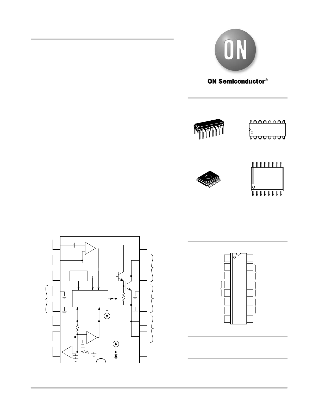
The MC34163 series are monolithic power switching regulators that
contain the primary functions required for dc−to−dc converters. This
series is specifically designed to be incorporated in step−up,
step−down, and voltage−inverting applications with a minimum
number of external components.
These devices consist of two high gain voltage feedback
comparators, temperature compensated reference, controlled duty
cycle oscillator, driver with bootstrap capability for increased
efficiency, and a high current output switch. Protective features consist
of cycle−by−cycle current limiting, and internal thermal shutdown.
Also included is a low voltage indicator output designed to interface
with microprocessor based systems.
These devices are contained in a 16 pin dual−in−line heat tab plastic
package for improved thermal conduction.
Features
• Output Switch Current in Excess of 3.0 A
• Operation from 2.5 V to 40 V Input
• Low Standby Current
• Precision 2% Reference
• Controlled Duty Cycle Oscillator
• Driver with Bootstrap Capability for Increased Efficiency
• Cycle−by−Cycle Current Limiting
• Internal Thermal Shutdown Protection
• Low Voltage Indicator Output for Direct Microprocessor Interface
• Heat Tab Power Package
• Moisture Sensitivity Level (MSL) Equals 1
• Pb−Free Packages are Available*
16
9
10
11
12
13
14
15
8
7
6
5
4
3
2
Control Logic
and Thermal
Shutdown
LVI
OSC
+
+
−
Voltage
Feedback 2
Voltage
Feedback 1
GND
Timing
Capacitor
V
CC
I
pk
Sense
Bootstrap
Input
Switch
Emitter
GND
Switch
Collector
Driver
Collector
+
+
+
I
Limit
VFB
Figure 1. Representative Block Diagram
(Bottom View)
−
+
+
+
−
1
LVI Output
This device contains 114 active transistors.
116
15
14
13
12
11
10
9
2
3
4
5
6
7
8
(Top View)
LVI Output
Voltage Feedback 2
Voltage Feedback 1
GND
Timing Capacitor
V
CC
I
pk
Sense
Bootstrap Input
Switch
Emitter
GND
Switch Collector
Driver Collector
PIN CONNECTIONS
See detailed ordering and shipping information in the package
dimensions section on page 2 of this data sheet.
ORDERING INFORMATION
MARKING
DIAGRAMS
x = 3 or 4
A = Assembly Location
WL = Wafer Lot
YY = Year
WW = Work Week
G = Pb−Free Package
PDIP−16
P SUFFIX
CASE 648C
1
16
SOIC−16W
DW SUFFIX
CASE 751G
http://onsemi.com
16
1
MC3x163DW
AWLYYWWG
16
1
MC3x163P
AWLYYWWG
16
1
*For additional information on our Pb−Free strategy
and soldering details, please download the
ON Semiconductor Soldering and Mounting
Techniques Reference Manual, SOLDERRM/D.
器件 Datasheet 文档搜索
AiEMA 数据库涵盖高达 72,405,303 个元件的数据手册,每天更新 5,000 多个 PDF 文件
