Datasheet 搜索 > 微控制器 > Freescale(飞思卡尔) > MC68HC908QY1CP 数据手册 > MC68HC908QY1CP 产品封装文件 5/184 页

 器件3D模型
¥ 0
MC68HC908QY1CP 产品封装文件 - Freescale(飞思卡尔)
制造商:
Freescale(飞思卡尔)
分类:
微控制器
封装:
DIP-16
Pictures:
3D模型
符号图
焊盘图
引脚图
产品图
页面导航:
引脚图在P19P21P22P100P101P102Hot
原理图在P19P20P42P43P50P57P74P75P80P81P85P90
封装尺寸在P165
型号编码规则在P165
功能描述在P17P18P20P22P24P41P43P49P53P55P57P73
技术参数、封装参数在P92P93P149P150P152P154P156P158P160P162P164P165
应用领域在P96
电气规格在P86P92P93P149P150P151P152P154P155P156P158P160

导航目录
MC68HC908QY1CP数据手册
Page:
of 184 Go
若手册格式错乱,请下载阅览PDF原文件
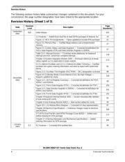
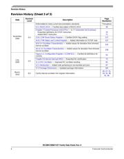
MC68HC908QY/QT Family Data Sheet, Rev. 6
Freescale Semiconductor 5
August,
2003
1.0
Reformatted to meet latest M68HC08 documentation standards N/A
Figure 1-1. Block Diagram — Diagram redrawn to include keyboard interrupt
module and TCLK pin designator.
20
Figure 1-2. MCU Pin Assignments — Added TCLK pin designator. 21
Table 1-2. Pin Functions — Added TCLK pin description. 22
Table 1-3. Function Priority in Shared Pins — Revised table for clarity and to
add TCLK.
23
Figure 2-1. Memory Map — Corrected names for the IRQ status and control
register (INTSCR) bits 3–0.
26
3.7.3 ADC Input Clock Register — Clarified bit description for the ADC clock
prescaler bits.
47
4.3 Functional Description — Updated periodic wakeup request values. 51
Figure 6-1. COP Block Diagram — Reworked for clarity 59
Chapter 8 External Interrupt (IRQ) — Corrected bit names for MODE, IRQF,
ACK, and IMASK
77–79
Chapter 14 Timer Interface Module (TIM) — Added TCLK function. 131–139
15.3 Monitor Module (MON) — Updated with additional data. 147
Chapter 16 Electrical Specifications — Updated with additional data. 169–173
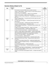
October,
2003
2.0
Figure 2-2. Control, Status, and Data Registers — Deleted unimplemented
areas from $FFB0–$FFBD and $FFC2–$FFCF as they are actually available.
Also corrected $FFBF designation from unimplemented to reserved.
27
Figure 6-1. COP Block Diagram — Reworked for clarity 59
6.3.2 STOP Instruction — Added subsection 60
13.4.2 Active Resets from Internal Sources — Reworked notes for clarity. 111
Table 13-2. Reset Recovery Timing — Replaced previous table with new
information.
112
Chapter 14 Timer Interface Module (TIM) — Updated with additional data. 131
Figure 15-3. Break I/O Register Summary — Corrected bit designators for the
BRKAR register
143
15.3 Monitor Module (MON) — Clarified seventh bullet. 147
Table 17-1. MC Order Numbers — Corrected temperature and package
designators.
175
January,
2004
3.0
Figure 2-2. Control, Status, and Data Registers — Corrected reset state for the
FLASH Block Protect Register at address location $FFBE and the Internal
Oscillator Trim Value at $FFC0.
32
Figure 2-5. FLASH Block Protect Register (FLBPR) — Restated reset state for
clarity.
38
Revision History (Sheet 2 of 3)
Date
Revision
Level
Description
Page
Number(s)
器件 Datasheet 文档搜索
AiEMA 数据库涵盖高达 72,405,303 个元件的数据手册,每天更新 5,000 多个 PDF 文件
