Datasheet 搜索 > 接口芯片 > ON Semiconductor(安森美) > MC74HC4053ADTR2G 数据手册 > MC74HC4053ADTR2G 其他数据使用手册 1/18 页

 器件3D模型
¥ 0.856
MC74HC4053ADTR2G 其他数据使用手册 - ON Semiconductor(安森美)
制造商:
ON Semiconductor(安森美)
分类:
接口芯片
封装:
TSSOP-16
描述:
2通道模拟复用/分配器
Pictures:
3D模型
符号图
焊盘图
引脚图
产品图
页面导航:
典型应用电路图在P2P3
封装尺寸在P14P15P16P17
焊盘布局在P14P15P16P17
型号编码规则在P1P13P18
标记信息在P1P14P16P17P18
封装信息在P13
技术参数、封装参数在P13
应用领域在P1P10P13
型号编号列表在P3
导航目录
MC74HC4053ADTR2G数据手册
Page:
of 18 Go
若手册格式错乱,请下载阅览PDF原文件
© Semiconductor Components Industries, LLC, 2017
April, 2021 − Rev. 11
1 Publication Order Number:
MC74HC4051A/D
Analog Multiplexers/
Demultiplexers
High−Performance Silicon−Gate CMOS
MC74HC4051A,
MC74HC4052A,
MC74HC4053A
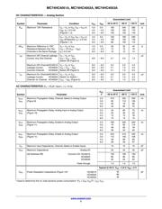
The MC74HC4051A, MC74HC4052A and MC74HC4053A utilize
silicon−gate CMOS technology to achieve fast propagation delays,
low ON resistances, and low OFF leakage currents. These analog
multiplexers/demultiplexers control analog voltages that may vary
across the complete power supply range (from V
CC
to V
EE
).
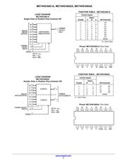
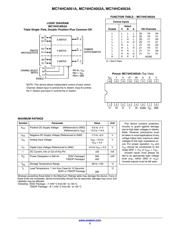
The HC4051A, HC4052A and HC4053A are identical in pinout to
the metal−gate MC14051AB, MC14052AB and MC14053AB. The
Channel−Select inputs determine which one of the Analog
Inputs/Outputs is to be connected, by means of an analog switch, to the
Common Output/Input. When the Enable pin is HIGH, all analog
switches are turned off.
The Channel−Select and Enable inputs are compatible with standard
CMOS outputs; with pullup resistors they are compatible with LSTTL
outputs.
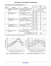
These devices have been designed so that the ON resistance (R
on
) is
more linear over input voltage than R
on
of metal−gate CMOS analog
switches.
For a multiplexer/demultiplexer with injection current protection,
see HC4851A and HC4852A.
Features
• Fast Switching and Propagation Speeds
• Low Crosstalk Between Switches
• Diode Protection on All Inputs/Outputs
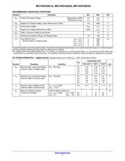
• Analog Power Supply Range (V
CC
− V
EE
) = 2.0 to 12.0 V
• Digital (Control) Power Supply Range (V
CC
− GND) = 2.0 to 6.0 V
• Improved Linearity and Lower ON Resistance Than Metal−Gate
Counterparts
• Low Noise
• In Compliance with the Requirements of JEDEC Standard No. 7A
• Chip Complexity: HC4051A − 184 FETs or 46 Equivalent Gates
HC4052A − 168 FETs or 42 Equivalent Gates
HC4053A − 156 FETs or 39 Equivalent Gates
• NLV Prefix for Automotive and Other Applications Requiring
Unique Site and Control Change Requirements; AEC−Q100
Qualified and PPAP Capable
• These Devices are Pb−Free, Halogen Free/BFR−Free and are RoHS
Compliant
This document contains information on some products that are still under development.
ON Semiconductor reserves the right to change or discontinue these products without
notice.
www.onsemi.com
MARKING DIAGRAMS
SOIC−16
TSSOP−16
1
16
HC405xAG
AWLYWW
HC40
5xA
ALYWG
G
1
16
SOIC−16 WIDE
1
16
HC405xA
AWLYWWG
See detailed ordering and shipping information in the package
dimensions section on page 13 of this data sheet.
ORDERING INFORMATION
x = 1, 2 or 3
A = Assembly Location
WL, L = Wafer Lot
YY, Y = Year
WW, W = Work Week
G or G = Pb−Free Package
(Note: Microdot may be in either location)
SOIC−16
D SUFFIX
CASE 751B
TSSOP−16
DT SUFFIX
CASE 948F
SOIC−16 WIDE
DW SUFFIX
CASE 751G
4051
ALYWG
G
QFN16
1
QFN16
MN SUFFIX
CASE 485AW
器件 Datasheet 文档搜索
AiEMA 数据库涵盖高达 72,405,303 个元件的数据手册,每天更新 5,000 多个 PDF 文件
