Datasheet 搜索 > 锁存器 > ON Semiconductor(安森美) > MC74HC573ADT 数据手册 > MC74HC573ADT 产品封装文件 1/7 页
 器件3D模型
¥ 0
MC74HC573ADT 产品封装文件 - ON Semiconductor(安森美)
制造商:
ON Semiconductor(安森美)
分类:
锁存器
封装:
TSSOP-20
描述:
八路三态同相透明锁存器 Octal 3-State Noninverting Transparent Latch
Pictures:
3D模型
符号图
焊盘图
引脚图
产品图
页面导航:
引脚图在P1Hot
典型应用电路图在P1P4
封装尺寸在P6P7
焊盘布局在P6
型号编码规则在P1P5P7
标记信息在P1P7
封装信息在P5
技术参数、封装参数在P5
应用领域在P1P5
电气规格在P2P3
型号编号列表在P2
导航目录
MC74HC573ADT数据手册
Page:
of 7 Go
若手册格式错乱,请下载阅览PDF原文件
© Semiconductor Components Industries, LLC, 2014
August, 2014 − Rev. 16
1 Publication Order Number:
MC74HC573A/D
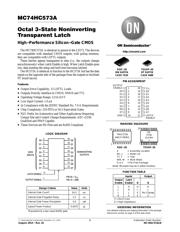
MC74HC573A
Octal 3-State Noninverting
Transparent Latch
High−Performance Silicon−Gate CMOS
The MC74HC573A is identical in pinout to the LS573. The devices
are compatible with standard CMOS outputs; with pullup resistors,
they are compatible with LSTTL outputs.
These latches appear transparent to data (i.e., the outputs change
asynchronously) when Latch Enable is high. When Latch Enable goes
low, data meeting the setup and hold time becomes latched.
The HC573A is identical in function to the HC373A but has the data
inputs on the opposite side of the package from the outputs to facilitate
PC board layout.
Features
• Output Drive Capability: 15 LSTTL Loads
• Outputs Directly Interface to CMOS, NMOS and TTL
• Operating Voltage Range: 2.0 to 6.0 V
• Low Input Current: 1.0 mA
• In Compliance with the JEDEC Standard No. 7.0 A Requirements
• Chip Complexity: 218 FETs or 54.5 Equivalent Gates
• NLV Prefix for Automotive and Other Applications Requiring
Unique Site and Control Change Requirements; AEC−Q100
Qualified and PPAP Capable
• These Devices are Pb−Free and are RoHS Compliant
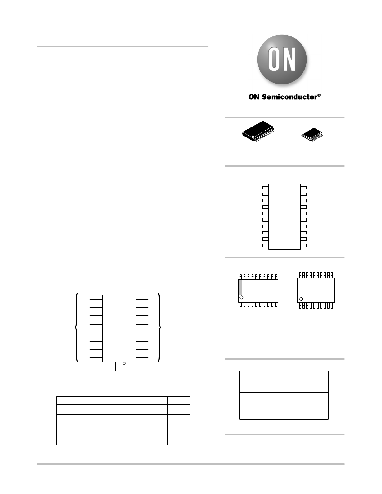
DATA
INPUTS
D0
D1
D2
D3
D4
D5
D6
D7
LATCH ENABLE
OUTPUT ENABLE
11
1
9
8
7
6
5
4
3
219
18
17
16
15
14
13
12
Q0
Q1
Q2
Q3
Q4
Q5
Q6
Q7
PIN 20 = V
CC
PIN 10 = GND
NONINVERTING
OUTPUTS
LOGIC DIAGRAM
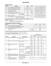
Design Criteria
*Equivalent to a two−input NAND gate.
Value Units
Internal Gate Count*
54.5 ea.
Internal Gate Progation Delay
1.5 ns
Internal Gate Power Dissipation
5.0 mW
Speed Power Product
0.0075 pJ
http://onsemi.com
1
20
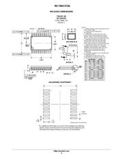
MARKING DIAGRAMS
SOIC−20
DW SUFFIX
CASE 751D
74HC573A
AWLYYWWG
HC
573A
ALYWG
G
TSSOP−20
DT SUFFIX
CASE 948E
20
1
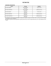
See detailed ordering and shipping information in the package
dimensions section on page 5 of this data sheet.
ORDERING INFORMATION
A = Assembly Location
WL, L = Wafer Lot
YY, Y = Year
WW, W = Work Week
G or G = Pb−Free Package
(Note: Microdot may be in either location)
SOIC−20 TSSOP−20
D4
D2
D1
D0
OUTPUT
ENABLE
GND
D7
D6
D5
D3 5
4
3
2
1
10
9
8
7
6
14
15
16
17
18
19
20
11
12
13
Q3
Q2
Q1
Q0
V
CC
LATCH
ENABLE
Q7
Q6
Q5
Q4
PIN ASSIGNMENT
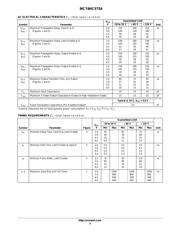
FUNCTION TABLE
Inputs Output
Output Latch
Enable Enable D Q
LHHH
LHLL
L L X No Change
HXXZ
X = Don’t Care
Z = High Impedance
器件 Datasheet 文档搜索
AiEMA 数据库涵盖高达 72,405,303 个元件的数据手册,每天更新 5,000 多个 PDF 文件
